
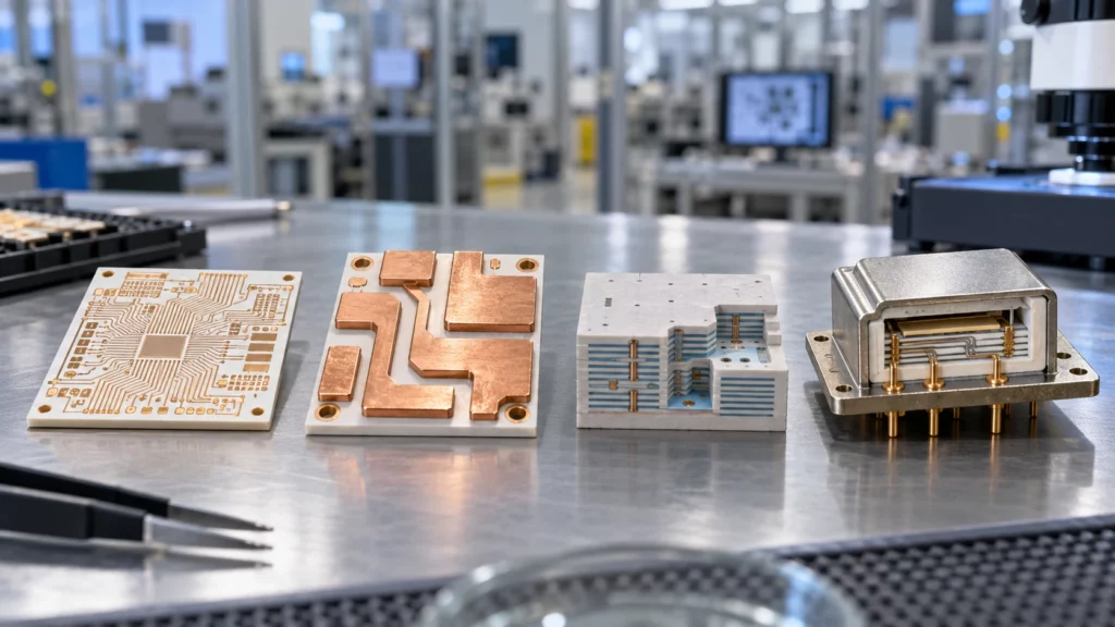
DPC, DBC, LTCC, and HTCC are not interchangeable versions of the same ceramic PCB. DPC and DBC add copper to a fired substrate. LTCC and HTCC build conductors, vias, and ceramic layers together before co-firing. Use DPC for fine surface features, DBC for thick copper and heat spreading, LTCC for compact multilayer integration, and HTCC for very high operating temperatures or demanding hermetic service.
The final choice also depends on substrate material, copper thickness, circuit density, package geometry, operating conditions, and volume. Match the manufacturing route to the functions the ceramic must perform.
The first decision is surface metallization or co-fired construction
First ask whether the design needs a circuit on a finished ceramic plate or an integrated body with buried features. DPC and DBC are post-fired routes that create copper circuitry on pre-fired alumina or aluminum nitride. They fit many power, LED, laser, and RF assemblies where ceramic provides insulation, stability, and a short heat path.
LTCC and HTCC begin with unfired ceramic tapes. Patterned layers are laminated, then ceramic and metallization are fired together. This enables buried routing, cavities, channels, and compact three-dimensional packages. The Fraunhofer IKTS overview of LTCC and HTCC highlights multilayer integration, hermetic sealing, high-frequency performance, and temperature stability.
How the four ceramic PCB processes differ
Compare how metal is added, the conductor structure each route favors, and whether multilayer integration is inherent. The table shows the normal design fit; final limits require manufacturer confirmation.
| Process | How the circuit is formed | Best design fit | Main tradeoff |
| DPC | A thin metal seed layer is patterned, then copper is built by plating on fired ceramic. | Fine lines, small pads, moderate copper, prototypes, RF and optical assemblies | Less suitable than DBC when very thick copper is the main requirement. |
| DBC | Copper foil is directly bonded to fired ceramic at elevated temperature and then patterned. | High current, power modules, strong heat spreading, larger copper features | Thick copper makes fine etching and dense routing more difficult. |
| LTCC | Printed conductor layers and vias are laminated in ceramic glass tapes and co-fired. | Compact multilayers, embedded passives, RF modules, sensors, cavities and channels | Material system and shrinkage control constrain dimensions and conductor choices. |
| HTCC | Refractory metal conductors and ceramic layers are laminated and co-fired at higher temperatures. | Hermetic packages, harsh environments, high-temperature electronics, and robust feedthroughs | Higher firing temperature limits conductor systems and can add post-fire finishing steps. |
DPC for fine surface features and controlled copper buildup
DPC is a strong starting point for relatively fine lines, small pads, or accurate surface geometry on alumina or aluminum nitride. A deposited seed layer, imaging, and electroplating allow you to build copper after patterning. It suits sensor carriers, optoelectronic modules, RF circuits, and compact power devices that don’t need DBC-style heavy copper. Specify finished copper thickness because plating affects current capacity and achievable spacing.
DBC for thick copper and heat spreading
DBC bonds comparatively thick copper directly to ceramic. It suits IGBT, SiC, GaN, inverter, charger, and high-power LED structures where heat spreading and current handling outweigh routing density. Check copper thickness, isolation distance, copper balance, edge clearance, and the heat-sink interface. If the board also needs very fine traces, dense pads, or buried routing, thick copper can become the limiting factor.
LTCC for compact multilayer integration
LTCC fits packages that integrate routing layers, vias, passive elements, cavities, or fluidic features. Its lower co-firing temperature supports conductor systems used in compact RF front ends, sensors, and microwave modules. Designers must account for tape shrinkage, dielectric behavior, via geometry, and the fact that ceramic and metal are qualified as one system. A material change can require broader requalification.
HTCC for high-temperature and hermetic packages
HTCC uses higher firing temperatures and refractory metallization systems to form a dense multilayer body. It is considered for hermetic packages, feedthroughs, sensors, and electronics exposed to high temperatures or aggressive environments. Compared with LTCC, it trades conductor and integration options for a different temperature and material window. It adds value when the ceramic body, internal conductors, and sealed package function as one structure.
Where each process is used in practice
Process names are easier to judge when tied to products. The four routes dominate different corners of the ceramic PCB market, and knowing where each one is already proven shortens the selection debate considerably.
DPC in practice. Direct plated copper appears most often in RF and optical assemblies, sensor packages, LED substrates, and thermal test boards where fine surface features matter more than copper mass. Because tooling is comparatively light, DPC also carries a large share of prototype and low-volume ceramic work, including design verification builds that run before a thicker copper route is committed.
DBC in practice. Bonded copper dominates power electronics: EV traction inverters, on-board chargers, solar string inverters, industrial motor drives, and the IGBT or SiC modules inside them. Any design that combines high current with a requirement to pull heat through the substrate usually lands on DBC, and it remains the default when copper is measured in tenths of a millimeter rather than microns.
LTCC in practice. Co-fired tape suits compact multilayer integration: automotive radar front ends, RF and millimeter wave modules, implantable medical devices, MEMS sensor packages with cavities or channels, and avionics assemblies that benefit from buried passives in a small footprint. It is also a common choice when a design has to combine electrical routing with fluidic or mechanical features in a single body.
HTCC in practice. Refractory metallization serves the harshest environments: hermetic sensor and detector packages, downhole electronics for oil and gas, aerospace and defense hardware, high-temperature automotive sensors, and microwave tube assemblies. When a package must survive hundreds of degrees, maintain vacuum tightness, or tolerate repeated thermal shock, HTCC is often the only practical ceramic route.
Cost drivers: how the four processes compare
Ceramic PCB cost is usually discussed as a single number, which hides the fact that the four processes spend money in different places. At prototype volume, tooling, setup, and inspection dominate; at production volume, yield, panel utilization, and finishing steps take over.
| Process | Where cost concentrates at prototype volume | Where cost concentrates at production volume |
| DPC | Photolithographic patterning, plating setup, fine feature inspection | Plating uniformity across panels, fine line yield, inspection time |
| DBC | Copper bonding process setup, etching of thick copper | Copper utilization, thick copper etch yield, panel size limits |
| LTCC | Tape tooling, lamination and co-firing setup, shrinkage compensation | Layer count, via and cavity yield, cost per tape layer |
| HTCC | High temperature firing setup, refractory metallurgy, finishing operations | Firing energy and yield, hermeticity testing, post-fire plating |
A practical consequence is that prototype quotations say very little about production price. A route with low setup cost can become the expensive one once layer counts, copper thickness, or hermeticity requirements scale up. Comparisons only become meaningful when both volumes are quoted against the same stack-up, panel size, and inspection level.
This is why UMEC reviews ceramic PCB projects in two stages: a prototype quotation covering tooling, setup, and a small build, and a production model that projects yield, panel utilization, and test cost at the target volume. Reviewing both before committing to a process avoids the common situation where a route that worked for the pilot turns out to be the wrong one for volume.
Common process selection mistakes
Choosing a process before ranking the load. Thick copper, fine lines, and hermeticity rarely coexist comfortably in one design. A project that selects DBC for its power handling and then asks for very fine lines creates an unnecessary conflict; ranking the dominant load first usually removes the contradiction before it reaches layout.
Treating LTCC and HTCC as premium versions of DPC and DBC. Co-fired routes change the material system, the shrinkage behavior, and the available conductor choices. Design rules carried over from a surface-metalized substrate will not transfer without revision, and the cost of discovering this during co-firing is measured in tooling, not redraws.
Comparing quotations built on different assumptions. A ceramic quotation is only comparable when stack-up, copper thickness, minimum features, panel size, and inspection criteria match. Quotations prepared under different assumptions produce different numbers for the same design, which makes the cheaper offer the riskier one.
Die attach, wire bonding, soldering, heat-sink contact, and hermetic testing all constrain the ceramic choice. A process that fits the circuit but not the assembly sequence still fails, and it fails later, after tooling has been paid for. For that reason, UMEC reviews the assembly and test sequence with the circuit before releasing ceramic tooling.
None of these mistakes are expensive to avoid at the drawing stage. Almost all of them become expensive once tooling is cut and material is committed.
A selection workflow for real designs
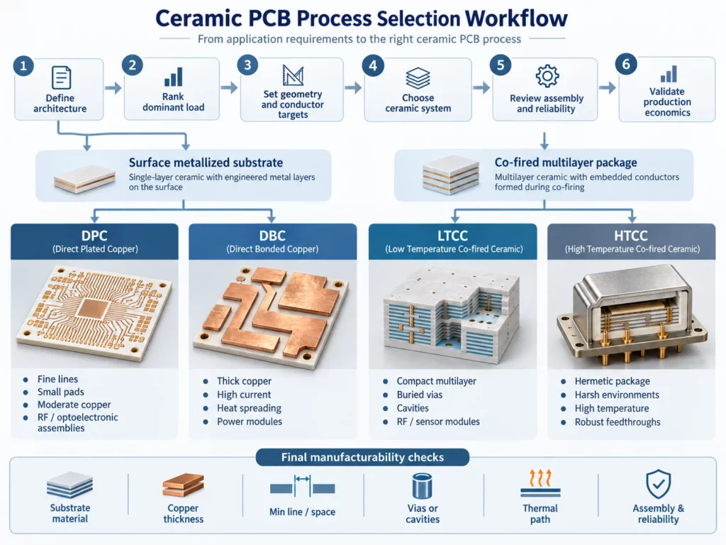
- Define the architecture. Choose between a surface-metalizedsubstrate and a co-fired multilayer package before comparing line width or cost.
- Rank the dominant load. State whether the design is limited by current, heat flux, RF loss, isolation voltage, operating temperature, or package size.
- Set geometry and conductor targets. Provide minimum line and space, copper thickness, pad size, via structure, board dimensions, and any buried layers or cavities.
- Choose the ceramic system. Alumina, aluminum nitride, silicon nitride, and proprietary LTCC or HTCC tapes have different thermal, mechanical, dielectric, and processing behavior.
- Review assembly and reliability. Include die attach, soldering or wire bonding, heat-sink contact, thermal cycling, hermeticity, surface finish, and inspection requirements.
- Validate production economics. Compare tooling, panel utilization, process yield, inspection, and volume. A low unit price is not useful if the process cannot hold the required geometry or reliability window.
Material and geometry still control manufacturability.
A process label cannot be separated from its design limits. UMEC’s published ceramic PCB capability table lists alumina and aluminum nitride among standard materials, DPC plus electroplating, advanced line and space down to 0.8/0.8 mil, outer copper up to 28 oz, and advanced laser drilling down to 0.06 mm. These are separate limits, not a promise that every extreme can be combined in one build.
Request a stack-up-specific DFM review. Copper thickness changes etching and spacing; ceramic thickness and board size affect handling and flatness. The manufacturer should confirm which limits apply simultaneously.
What to send suppliers before process selection
Send Gerber or ODB++ data, a mechanical drawing, substrate and copper specifications, minimum features, hole chart, surface finish, operating conditions, cooling method, assembly process, reliability tests, and volume. If the architecture is still open, a PCB design and layout review can show whether the structure points toward DPC, DBC, LTCC, or HTCC.
Supplier evaluation should cover material traceability, metallization control, dimensional and electrical testing, surface finish, and controls for cracks, warpage, and copper defects. Review the manufacturer’s quality assurance and inspection process and ask which checks apply to the selected route and production acceptance criteria.
Conclusion
Choose DPC for fine surface circuitry, DBC for thick copper and heat spreading, LTCC for integrated multilayers, and HTCC for high-temperature or hermetic packages. Connect that choice to material, geometry, electrical load, thermal path, assembly, reliability, and volume.
Frequently asked questions
Can DPC replace DBC in a power module?
Sometimes. DPC favors finer features, but it must still meet copper thickness, current, heat-spreading, and thermal-cycling targets. DBC is the better starting point when thick copper defines the power path.
Is LTCC always better than HTCC for RF designs?
No. LTCC often suits compact RF multilayers, while HTCC may fit temperature stability, hermetic packaging, or environmental durability. Compare qualified material systems at the intended frequency and temperature.
Which ceramic PCB process supports the finest traces?
DPC commonly provides the finest surface patterning. Actual line and space depend on copper thickness, substrate, imaging, board size, and yield targets, so confirm the layout with the manufacturer.
Should the ceramic material be chosen before the process?
Choose them together. Alumina, aluminum nitride, silicon nitride, and co-fired tapes impose different thermal, mechanical, dielectric, metallization, and cost constraints.
Process fit check
For a project-specific decision, request a ceramic PCB process review from UMEC with the drawing, stack-up, substrate, copper thickness, minimum features, operating conditions, assembly method, reliability targets, and quantity.