
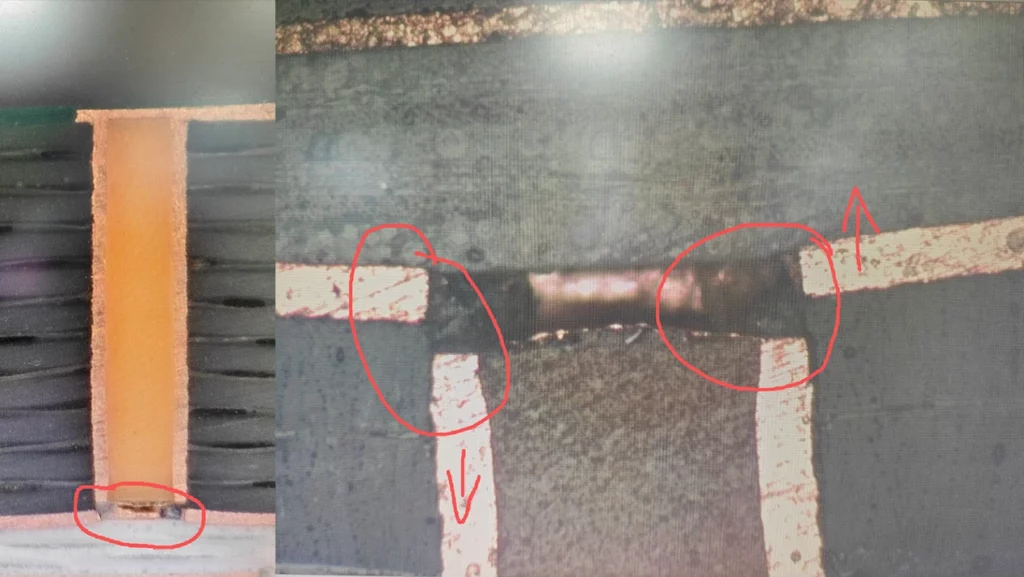
An HDI PCB can pass room-temperature electrical testing and still contain a latent microvia weakness that opens during reflow or repeated thermal cycling. For engineers investigating microvia failure, the key questions are where the interconnect is failing, what thermal or fabrication condition is exposing the weakness, and whether the inspection plan can detect it before production release. IPC has documented cases where microvia failures appeared only after reflow, environmental stress screening, or field use, even though the bare boards had already passed conventional acceptance testing.
Why Can a Microvia Pass Electrical Test but Fail After Reflow?
A continuity test at room temperature confirms that a conductive path exists at that moment; it does not prove that every microvia interface will remain stable through assembly temperatures and repeated thermal excursions.
A weak connection at the microvia-to-target interface may remain electrically continuous when cold. As the PCB heats, expansion within the copper, dielectric, and surrounding structure can place additional stress on that interface. An existing weakness may separate enough to create an open or resistance increase. Cooling can sometimes restore contact, making the defect intermittent and difficult to reproduce.
This is why a PCB that passes fabrication testing can fail during assembly. Reflow should not automatically be treated as the root cause: in some cases, it exposes a latent weakness already present in the HDI interconnect. IPC specifically warned that some microvia failures are undetectable at room temperature and emerge during later thermal exposure.
The Main HDI Microvia Failure Modes Engineers Need to Distinguish
Knowing that a microvia has failed is not enough. Failure location matters because interface separation, copper cracking, and plating defects point toward different corrective actions.
Weak Interface and Target-Pad Separation
One important failure mode occurs near the base of the microvia where deposited copper meets the target or capture pad. If that interface is weak, thermal expansion can progressively separate the connection until resistance increases or the circuit opens.
When a board passes a cold electrical test but fails hot, or becomes intermittent after reflow, the target interface deserves close investigation. Failure analysis needs to establish whether the separation is localized to one interface, repeated across a via chain, or concentrated within a particular HDI structure.
IPC technical work has documented target-pad-to-plating separation among observed microvia failure mechanisms. The practical next step is not to assume that every open is a drilling defect, but to correlate the electrical symptom with physical evidence from the affected interconnect.
Corner Cracks, Barrel Damage, and Plating Voids
Microvias can also exhibit barrel or corner cracking, while plating voids or incomplete copper formation may create local weak points. These conditions are different from target-interface separation, but all can become more significant when the structure is repeatedly heated and cooled.
A void visible in imaging does not automatically prove it caused the field failure. Likewise, a crack found in one destructive section does not establish the condition of every via on the panel. Engineers need to combine defect location, electrical behavior, thermal history, and physical inspection rather than rely on a single observation.
The objective is to move from “the microvia failed” to a defensible failure mechanism tied back to design, fabrication, or process control.
How Thermal Cycling Turns a Small Microvia Weakness Into an Open Circuit
CTE Mismatch, Z-Axis Stress, and Repeated Reflow
Copper and the materials surrounding an HDI microvia do not respond the same way to temperature changes. Reflow and thermal cycling repeatedly expand and contract the interconnect structure, which can accumulate mechanical strain at already weak interfaces or plated regions.
The risk depends on the complete construction: dielectric thickness, material system, microvia geometry, copper deposition, target-pad interface, stacked structure, and the thermal history expected during assembly and service. Microvia diameter alone is therefore not an adequate reliability metric.
Repeated thermal exposure is valuable in qualification because it can reveal weaknesses that static inspection misses. IPC’s microvia work emphasizes performance-based thermal testing and resistance monitoring to identify latent interconnect problems that may not be visible during conventional acceptance inspection.
How Does Stacked Microvia Structure Affect Reliability?
When Staggered Microvias Are Worth the Extra Routing Area
Stacked microvias support dense vertical interconnection, which can be valuable under fine-pitch components and in space-constrained HDI layouts. The tradeoff is that a stacked path depends on multiple vertically aligned interfaces, so the reliability assessment must consider the complete stack rather than one isolated microvia.
Staggered microvias use additional routing area but can be worth evaluating when a direct vertical stack provides little routing benefit relative to the reliability requirement. The decision depends on component escape needs, available board area, buildup structure, via filling, materials, and qualification requirements.
For fine-pitch designs where stacking is driven by BGA escape routing, UMEC’s HDI microvia design guidelines provide additional context on via-in-pad, stacked versus staggered structures, filling, and stackup choices.
The correct decision is not “stacked is bad” or “staggered is safe.” It depends on whether the chosen structure has enough routing value to justify its fabrication and reliability controls.
How Plating and Via Fill Affect Microvia Reliability
Target-Pad Preparation, Copper Deposition, and Via Fill Quality
Laser drilling creates the geometry, but reliable electrical connection depends on what happens afterward. Surface preparation at the target pad, copper deposition, adhesion, and fill quality all influence the finished microvia.
A weak target interface can become a thermal failure location, while voids or inconsistent fill can create regions where stress is less evenly distributed. In stacked structures, lower-level fill quality matters more because subsequent microvias depend on the underlying structure.
During supplier review, engineers must therefore ask how the specified microvia construction is formed, filled, inspected, and qualified rather than accepting “laser microvia capable” as sufficient evidence. UMEC publishes specific microvia/land, laser-drilling, aspect-ratio, and HDI buildup parameters under its HDI PCB manufacturing capabilities, which gives engineering teams a starting point for matching the design to a manufacturable structure.
How to Detect Latent Microvia Failure Before Production Release
What X-Ray and Microsection Can—and Cannot—Show
Inspection methods answer different questions. X-ray can provide useful structural information and reveal certain internal anomalies, while destructive microsectioning can expose plating interfaces, copper geometry, cracks, and other physical evidence at a selected location.
Neither method alone proves the reliability of every microvia. A microsection samples a particular location, and IPC has warned that traditional thermally stressed microsections evaluated with light microscopy alone may miss some microvia-to-target plating problems.
That limitation matters when the failure is thermally activated rather than continuously open. Visual evidence must therefore be interpreted alongside the electrical symptom and expected thermal environment. If the main concern is latent resistance change during heating, static structural inspection may need to be supplemented by a performance-based method.
When Thermal Stress, Resistance Monitoring, or IST Adds Better Evidence
Performance-based testing asks whether the interconnect remains electrically stable under stress. Thermal cycling with resistance monitoring can expose progressive or intermittent damage that a room-temperature continuity test may miss.
Interconnect Stress Testing, or IST, is one approach used for evaluating interconnect behavior under repeated thermal loading. The specific temperature range, cycle count, coupon construction, and acceptance threshold should be agreed upon based on the applicable specification and product reliability requirements, rather than assumed from a generic recipe.
IPC-6012F expanded its treatment of microvia reliability and includes coupon concepts intended for complex interconnected via structures. UMEC’s FAQ also states that its testing resources include IST testing and cross-sectioning, in addition to flying-probe and fixture electrical tests. This makes HDI PCB reliability testing a relevant discussion to have before the production acceptance plan is frozen.
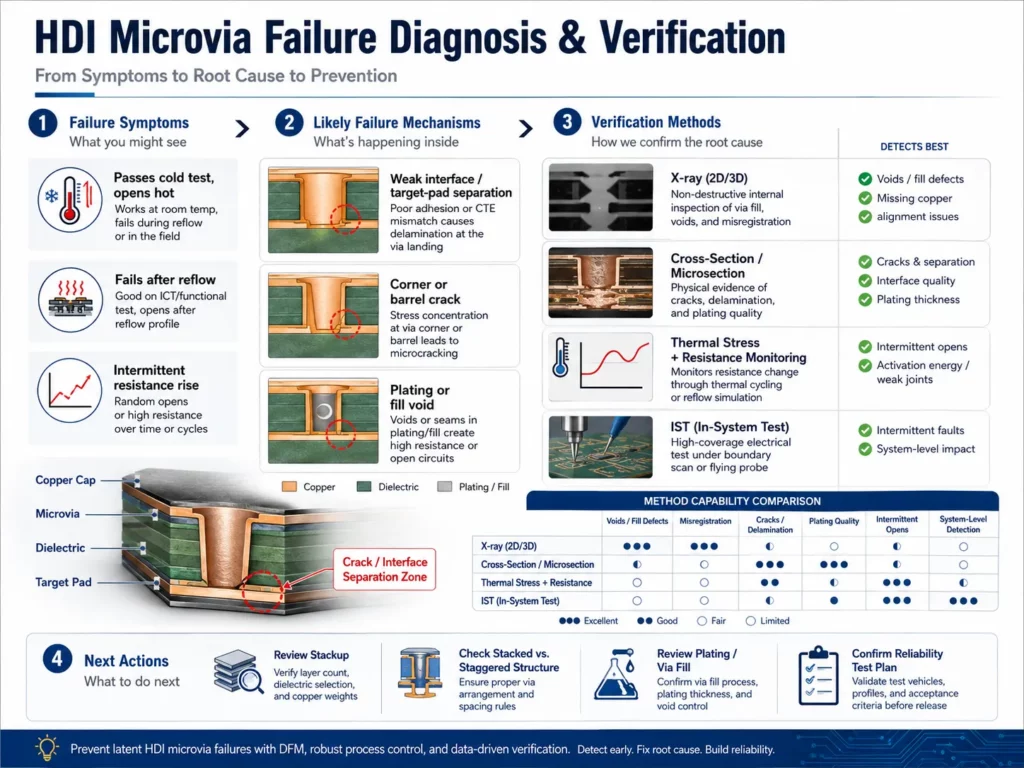
Microvia Failure Diagnosis Matrix
| Failure Symptom | Likely Investigation Direction | Verification Direction | Next Action |
| Passes cold test, opens when hot | Weak interface | Thermal resistance monitoring | Examine target-pad interface |
| Fails after repeated reflow | Fatigue or cracking | Thermal stress plus sectioning | Review structure and materials |
| Internal void observed | Plating or fill issue | Imaging plus sectioning | Review deposition and fill process |
| Failures cluster in stacked vias | Multiple-interface stress | Coupon testing plus sectioning | Reassess stack strategy |
| Intermittent resistance increase | Latent interconnect weakness | Performance-based testing | Isolate the failure via chain |
This matrix is a troubleshooting guide, not a substitute for failure analysis. The same electrical symptom can have multiple causes.
How to Prevent Microvia Failure Before the HDI Stackup Is Frozen
Remove Reliability Risk That Does Not Add Routing Value
Reliability prevention begins before you release production files. Review whether each stacked transition is actually required, whether the microvia and land geometry fit the manufacturer’s process window, and whether dielectric thickness and buildup structure create a sensible laser-drilling construction.
Do not add complex stacks merely because they fit the CAD layout. At the same time, do not convert a necessary high-density structure to a larger routing scheme if board area or signal requirements make that impractical.
Early DFM needs to connect routing density with material, via fill, buildup, reflow exposure, and qualification requirements. For broader fabrication and engineering support beyond the individual HDI product page, UMEC PCB manufacturing services provide the internal-link path from design review to fabrication and testing information.
What Should You Confirm With an HDI PCB Manufacturer Before RFQ?
Before requesting an HDI PCB quote, engineering and procurement must provide enough information to define the reliability scope, not just the Gerber package. Confirm the HDI buildup, microvia diameter and land, dielectric thickness, stacked or staggered structure, number of stacked interfaces, via-fill requirements, material, expected assembly/reflow exposure, operating environment, inspection scope, cross-section requirements, and any reliability coupon or thermal-test requirements.
Prototype and production acceptance plans also need to be distinguished. A prototype electrical test may confirm connectivity, while a reliability-critical production program may require additional application-specific evidence.
The goal is to prevent a supplier from pricing one scope while the buyer assumes another.
How to Choose an HDI PCB Supplier for Reliability-Critical Microvias
A supplier should be able to discuss process limits, not simply state that laser microvias are available. Buyers need to ask how the proposed stack is reviewed, how via filling and interfaces are controlled, what inspection methods are available, and how reliability requirements are reflected in the quotation.
SZ UMEC CO., LTD publishes HDI capabilities including laser-drilled hole limits, microvia/land geometry, laser aspect ratio, and electrical testing methods. Its FAQ further identifies IST and cross-sectioning among available testing resources.
For reliability-sensitive projects, those capabilities should still match the actual stackup and acceptance plan. A supplier qualification decision should be based on the specific construction, process controls, and agreed verification scope—not on a generic capability claim.
Conclusion
Microvia reliability cannot be demonstrated by room-temperature continuity alone. Failure prevention requires considering the design, plating process, thermal exposure, and inspection plan together before production release.
For an HDI project that needs reliability review, contact UMEC with the Gerber files, stackup, material, microvia structure, expected reflow conditions, operating environment, quantity, and required inspection or reliability criteria so the proposed build and test scope can be reviewed against the application.
HDI Microvia Failure FAQs
Why do microvias fail after reflow?
Reflow can expose an existing weak interface, crack, or plating defect because thermal expansion increases stress within the interconnect. Confirm the specific cause through electrical behavior and physical or performance-based testing.
Can a microvia pass electrical testing and still be defective?
Yes. IPC has documented latent microvia failures that passed conventional acceptance testing and appeared later during reflow, environmental stress, or field use.
Are stacked microvias more likely to fail during thermal cycling?
Reliability depends on stack construction, fill quality, interfaces, materials, thermal exposure, and qualification. More stacked interfaces may warrant additional review, but evaluate the structure as a complete design rather than judging it by stack count alone.
Is X-ray enough to check microvia reliability?
No single inspection method demonstrates every microvia failure mechanism. X-ray, microsectioning, electrical testing, thermal stress, and resistance-monitoring methods provide different evidence and may need to be combined for reliability-critical builds.