
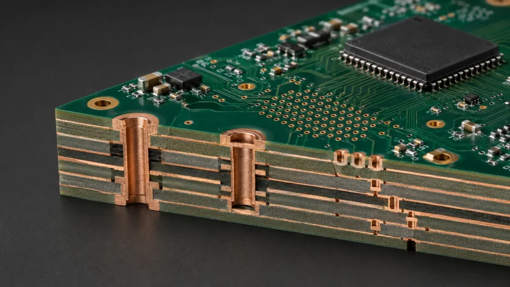
The selection among blind, buried, and micro vias for densely packed PCB designs is more than just an engineering decision. It affects the ease of routing, stackup design in HDI PCBs, PCB thickness, manufacturing costs, inspection issues, and reliability. In fact, for designers of fine-pitch BGA components, compact modules, high-speed traces, or size-constrained designs, having the right HDI via structure could avoid unnecessary layer additions and layout redesign. For purchasing people, it clarifies why two HDI PCB quotations can differ significantly even when they seem similar.
Why HDI Via Structure Matters in Dense PCB Designs
A traditional through-hole via runs through the whole board. This is very straightforward and often economical, but it also occupies routing space wherever it passes through. With HDI boards, particularly around BGA devices, through-hole vias can hinder the internal routes needed for proper signal escape, power distribution, and impedance-controlled traces.
HDI via structures solve this by connecting only the layers that need to be connected. Blind vias, buried vias, and microvias allow a PCB designer to use board space more efficiently, shorten certain interconnect paths, and support finer routing. The tradeoff is manufacturing complexity. More advanced via structures may require laser drilling, sequential lamination, via filling, tighter registration, and additional inspection.
When Through-Hole Vias Start Limiting Routing Freedom
However, through-hole vias will continue to be feasible if the component density is moderate, the BGA pitch is not very small, and there is sufficient room for trace routing around pads and vias. Through-hole vias pose a problem when the design consistently fails BGA fanout, requires too many layers, and the board outline keeps expanding.
This is often a good indication that the design already suffers from routing congestion even before the number of layers becomes too high. If more layers are required solely because through-hole vias interfere with escape, perhaps an HDI via structure will do better than simply adding layers. This decision must be made early, before the layout is finalized, since changing the stack-up later may affect impedance, materials, drilling specifications, and ultimately the quote.
Why Via Choice Affects Cost, Reliability and Supplier Review
Via choice changes the manufacturing flow. A simple through-hole structure is different from a board that uses blind and buried vias, filled microvias, or stacked microvias. Each added process step can affect cost and yield.
Reliability also depends on structure. A via that looks efficient in CAD may create plating, filling, or thermal stress concerns if it exceeds the supplier’s process window. Before prototyping or production, the design should be reviewed with the intended HDI PCB manufacturer to ensure the via span, stackup, materials, copper thickness, board thickness, and application environment are considered together.
Blind Vias, Buried Vias and Microvias: Key Differences for HDI PCB Design
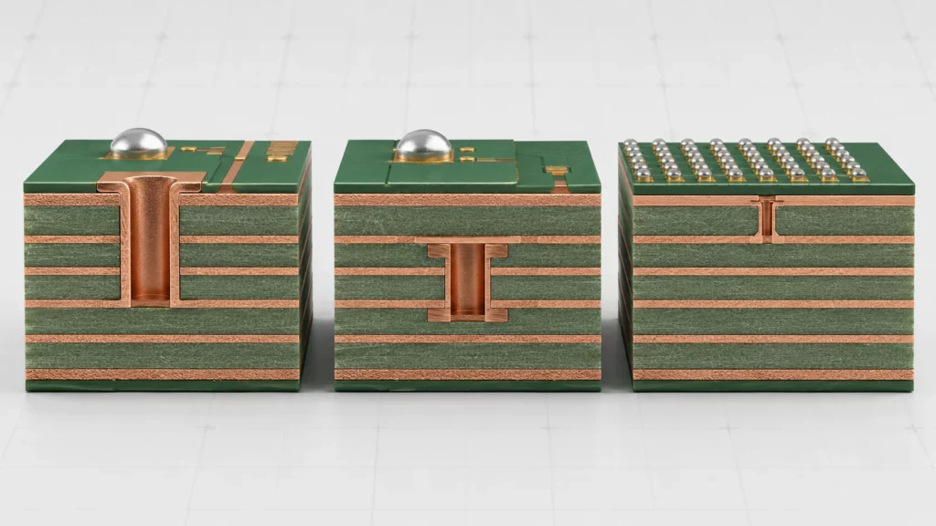
A blind via connects an outer layer to one or more internal layers without passing through the whole board. A buried via connects only internal layers and is not visible from the outside. A microvia is a small via, typically laser-drilled, often used between adjacent HDI layers for compact routing and fine-pitch escape.
| Via Type | Layer Connection | Typical Use | Cost Impact | Main Risk to Check |
| Blind via | Outer layer to inner layer | BGA escape, surface-to-inner routing | Medium to high | Depth, plating, registration |
| Buried via | Inner layer to inner layer | Internal routing density, freeing outer layers | Medium to high | Extra lamination and inspection |
| Microvia | Usually adjacent HDI layers | Fine-pitch BGA, compact HDI routing | Medium to high | Filling, stacking, reliability margin |
| Stacked microvia | Vertically aligned microvias | Maximum space saving | High | Thermal and plating stress |
| Staggered microvia | Offset microvias | Better manufacturing margin in many designs | Medium to high | Requires more layout space |
Blind Vias for Outer-to-Inner Layer Connections
Blind vias are useful when outer-layer components need access to internal routing layers without consuming space through the full PCB thickness. They are common in HDI PCB designs where BGA escape, compact modules, or dense surface routing make through-hole vias inefficient.
They are not automatically the right choice for every multilayer board. If routing can be completed with standard vias and an acceptable layer count, blind vias may add cost without enough benefit. During RFQ, buyers should confirm the start and stop layers by size, aspect ratio, board thickness, and whether the structure is mechanically or laser-drilled. These details help the supplier judge whether the design fits a stable fabrication window.
Buried Vias for Internal Routing Density
Buried vias are selected when internal layers need interconnection while keeping the outer layers open for components, traces, or microvia escape. They can be useful in dense boards where power, ground, and signal routing must be managed within the stackup.
The main tradeoff is process complexity. Because buried vias are formed before final lamination, they can add fabrication steps and inspection requirements. They are worth considering when internal routing density is a real constraint, but they should not be added only because they appear advanced. For procurement, the key question is whether buried vias reduce total design risk, layer count, or board size enough to justify the added process.
Microvias for Fine-Pitch and High-Density HDI Routing
Microvias are often used when fine-pitch BGA breakout, short interconnects, and compact routing are required. In many HDI designs, microvias connect adjacent layers such as L1 to L2 or L2 to L3. They may also be used with via-in-pad structures, depending on the design and manufacturing requirements.
Microvias are especially valuable when the design requires local routing density rather than full-board through connections. However, microvia PCB design should be reviewed carefully when vias are stacked, filled, or used across multiple HDI build-up layers. Filling method, pad design, material behavior, and thermal cycling requirements should be verified against the product specification and application conditions.
Level 1, Level 2, Level 3 and Any-Layer HDI: How Via Structure Changes
HDI level describes how many build-up layers or sequential microvia levels are used around the core. A 1+N+1 HDI stackup usually has one HDI build-up layer on each side of the core. A 2+N+2 stackup adds more HDI routing freedom, while 3+N+3 and Any-Layer HDI are used for more complex interconnect needs.
The right level depends on BGA pitch, pin count, board size, line width and spacing, impedance needs, and the acceptable cost range.
When 1+N+1 HDI Is Enough
A 1+N+1 HDI structure may be suitable when the design needs microvias for surface escape but does not require deep-stacked interconnections across many layers. It can support moderate HDI routing while keeping the structure less complex than higher-level HDI.
This option is worth checking first when the board has limited density pressure, controlled BGA breakout needs, or a cost target that does not support unnecessary lamination steps. It may not be enough if the design has very high-pin-count BGAs, tight board outline limits, or repeated routing congestion beyond the first HDI layer.
When 2+N+2 or 3+N+3 Becomes Necessary
A 2+N+2 or 3+N+3 structure becomes more relevant when a single level of microvias cannot provide sufficient routing channels. This may happen with fine-pitch BGAs, dense component placement, or compact products where increasing board size is not acceptable.
The decision should not be based only on routing convenience. More HDI levels may increase cost, process time, and reliability review requirements. Engineers should confirm whether stacked or staggered microvias are needed, whether via filling is required, and whether the same electrical goals could be met with a simpler structure.
When Any-Layer HDI Is Worth Considering
Any-Layer HDI offers greater routing freedom because microvias enable broad layer-to-layer interconnection throughout the stackup. It may be appropriate for very compact, high-density electronics where lower-level HDI cannot complete routing or meet size targets.
It is not the default choice for ordinary HDI boards. Any-Layer HDI should be considered when routing density, fine-pitch components, and space constraints justify the cost and manufacturing complexity. Before moving to this structure, the design should receive a DFM review from a supplier familiar with HDI PCB manufacturing capabilities.
Cost and Reliability Tradeoffs: Choosing the Practical Via Structure
HDI cost is often driven more by process steps than by board size alone. Sequential lamination, laser drilling, copper filling, stacked microvias, tighter line and space, and inspection requirements can all affect the quotation. A design with fewer layers but aggressive HDI features may cost more than a thicker board with simpler vias.
Reliability depends on how well the via structure matches the application. Stacked microvias can save space and shorten routing, but they require careful fabrication control. Staggered microvias may use more area, yet they can provide better process margin in many applications. The right answer depends on the operating environment, thermal exposure, board thickness, material, and assembly conditions.
HDI Via Structure Selection Matrix
| Design Condition | More Suitable Structure | Why It Fits | Risk to Check |
| Moderate density, outer-layer escape issue | Blind vias | Improves outer-to-inner routing | Via depth and plating margin |
| Dense internal routing | Buried vias | Frees surface layers | Lamination sequence and inspection |
| Fine-pitch BGA or compact module | Microvias | Supports short, dense interconnects | Via filling and pad design |
| Extreme routing freedom needed | Any-Layer HDI | Supports complex layer access | Cost, yield, supplier capability |
| Reliability-sensitive application | Staggered microvias where practical | Reduces stress concentration in many layouts | Extra layout space |
RFQ and DFM Checklist Before Finalizing HDI Via Structure
Before requesting an HDI PCB quote, prepare more than Gerber files. A useful RFQ should include the stackup target, BGA pitch, via type, via span, via-in-pad requirements, material preference, board thickness, copper weight, surface finish, quantity, application environment, and any reliability concerns.
The supplier should also know whether the project is for prototype verification, pilot build, or production. For complex boards, UMEC can review HDI PCB, PCB fabrication, PCB design and layout, component sourcing, PCB assembly, and testing needs as part of a broader project discussion.
Key DFM questions include:
- Can the proposed HDI level be manufactured within a stable process window?
- Are stacked microvias necessary, or can staggered microvias reduce risk?
- Does the design require via filling, copper filling, or special pad treatment?
- Are the selected material and board thickness suitable for the via structure?
- What files or drawings are needed for a more accurate quotation?
How to Choose an HDI PCB Supplier for Blind, Buried and Microvia Designs
A qualified HDI PCB supplier should help buyers and engineers connect design intent with manufacturable structure. The supplier should be able to discuss via span, HDI level, microvia design, stackup feasibility, routing density, material compatibility, and production risk before the design reaches the factory floor.
For projects involving blind vias, buried vias, microvias, or Any-Layer HDI, supplier selection should not focus only on the lowest unit price. A lower quote may not reflect the same stackup, filling method, inspection plan, or reliability margin. The safer approach is to request DFM feedback early and compare quotations based on the same technical assumptions.
UMEC supports customers through PCB fabrication and broader electronics manufacturing services. For projects that require more than board production, PCBを超える highlights the roles of design support, component sourcing, PCB assembly, and testing in helping buyers move from design files to finished electronic products.
Conclusion
Choosing between blind vias, buried vias, and microvias is a practical engineering decision. Blind vias help with outer-to-inner routing, buried vias improve internal routing density, and microvias support fine-pitch HDI layouts where compact interconnects are required. Higher-level HDI and Any-Layer HDI can provide more routing freedom, but they should be selected only when the density, reliability, and cost tradeoffs make sense.
For a reliable quotation or DFM review, submit Gerber or ODB++ files, stackup, BGA pitch, via structure, board size, material, surface finish, quantity, and application requirements. Buyers and engineers can contact UMEC to discuss HDI PCB fabrication details before finalizing prototype or production decisions.
FAQs
How does a blind via differ from a buried via and a microvia?
A blind via connects the external and internal layers, while a buried via connects only internal layers. A microvia is a small via used in HDI PCB design, typically fabricated by laser drilling and routed between adjacent layers.
When should a microvia be used over a blind or buried via in a PCB design?
Normally, microvias are chosen when fine-pitch BGA breakout, routing, or short interconnections between layers are required. Still, the final decision will depend on pitch, number of layers, board size, material, and your supplier’s capabilities.
Are buried vias more expensive than blind vias?
Buried vias can increase cost because they may require internal drilling, plating, lamination, and inspection before the full board is built. Actual cost depends on stackup, quantity, via count, and manufacturing process.
Are stacked microvias reliable for HDI PCB designs?
Stacked microvias can be reliable when the structure, filling, material, and process control are suitable for the application. For reliability-sensitive designs, stacked and staggered options should be reviewed during DFM.
When is Any-Layer HDI PCB worth the extra cost?
Any-Layer HDI is worth considering when lower-level HDI structures cannot meet routing density, board size, or fine-pitch component requirements. It should be verified with the supplier before layout is finalized.