
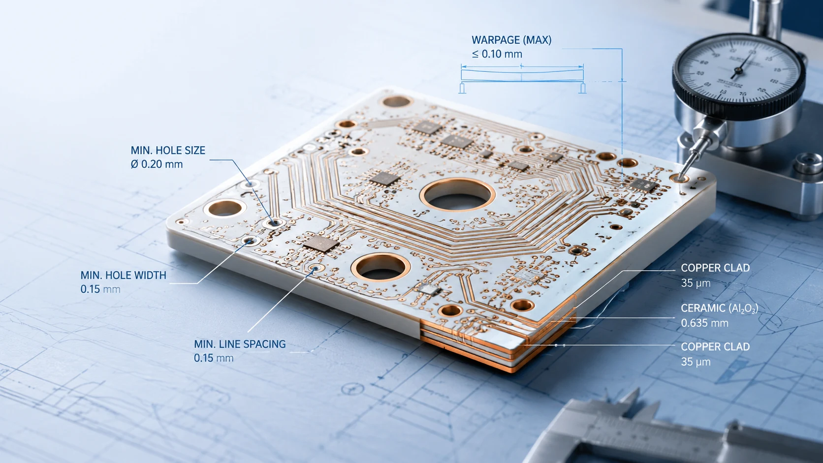
Design rules for ceramic PCB are most critical when your PCB needs to dissipate heat, conduct current or voltage, or handle high frequencies in a size-restricted area. If you do not have an initial review of your design based on parameters such as hole size, line/space, copper weight, edge clearance, and flatness, transitioning a working design for FR4 to a ceramic board might become challenging and costly. It is important not just to make your ceramic PCB manufacturability-friendly but also to prevent failures such as cracks, yield issues, assembly problems, delayed quotes, and unnecessary redesigns. UMEC will provide you with support from design to manufacturing.
Quick Ceramic PCB DFM Checklist Before You Send Gerber Files
Before sending Gerber files for a ceramic PCB quote, the first question is simple: Does the design match the ceramic material, copper structure, process, and inspection requirements?
For a meaningful DFM assessment of ceramic PCBs, the substrate material, thickness of the board, board dimensions, copper thickness, minimum line width, minimum space between the lines, size of the holes, tolerance for holes, surface finish, treatment of vias, flatness requirement, and the intended use of the PCB must all be verified. In addition, for high-power LED modules, electric vehicle power electronics, IGBT modules, lasers, RF front ends, and sensors, temperature, current, insulating requirements, and mounting should be provided.
Whenever possible, provide the manufacturer with Gerber or ODB++ files, mechanical drawings, material preferences (such as alumina or aluminum nitride), copper thickness, surface finish, intended volume, and application. This will help you transition more quickly from a general inquiry about ceramic PCB to an engineering review, which will support the quotation and production planning process.
Why Ceramic PCB Design Rules Are Different from FR4 PCB Rules
FR4 is a glass-reinforced laminate. Materials such as alumina (Al₂O₃), aluminum nitride (AlN), silicon nitride (SiN), silicon carbide (SiC), zirconium oxide (ZrO₂), sapphire, and ZTA exhibit different properties in operations such as drilling, metallization, wiring, welding, and assembly. Ceramics can provide good thermal conductivity, insulation, temperature stability, and dimensional stability, but are more rigid and fragile than FR4.
That is why DFM design rules for ceramic PCBs should consider the substrate as a part of a mechanical and thermal system, not only as an electrical insulator.
Ceramic Substrates Are Hard, Brittle, and Less Forgiving Than FR4
Ceramic substrates are less tolerant of aggressive mechanical stress. Small holes, narrow edge clearances, sharp internal corners, unbalanced copper, and tight mounting pressure can increase the risk of cracking, chipping, or warpage.
This does not mean ceramic PCBs are fragile in use. In the right application, they can be highly reliable. The issue is that the design must respect how ceramic materials are drilled, cut, plated, bonded, and assembled. A good ceramic PCB design guide should therefore include both mechanical and electrical rules.
Thermal Conductivity Helps Heat Dissipation, But It Does Not Remove Layout Constraints
One of the key properties of ceramic PCBs that engineers consider is their high thermal conductivity. Usually, alumina is chosen as a compromise between cost and insulating properties, whereas aluminum nitride is used when higher thermal conductivity is needed. Nevertheless, thermal conductivity solves only some heat-related issues.
Heat must be distributed through the copper, solder joint, ceramic substrate, thermal interface material, mounting surface, and heat sink anyway. A thin trace, an improper copper ratio, insufficient surface area, or non-uniform pressure during mounting can lead to hot spots. For that reason, ceramic PCB design rules should connect thermal design with copper thickness, trace width, pad size, via strategy, and assembly method.
Minimum Hole Size Rules for Ceramic PCB
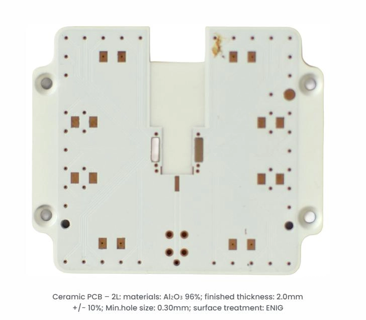
Hole design affects more than the electrical connection. It can influence plating reliability, metallization quality, board strength, routing yield, and assembly alignment. For ceramic PCB fabrication, the minimum hole size should be checked with the manufacturer before layout release, especially when the design uses dense pads, fine traces, or laser-drilled vias.
Mechanical Drilling vs Laser Drilling: Which One Should You Use?
Mechanical drilling is typically used for larger holes, mounting holes, and conventional through-hole structures. Laser drilling is more suitable for small vias and higher-density ceramic PCB designs where mechanical tools may not be practical.
UMEC ceramic PCB capabilities previously confirmed in this project include mechanical drilling and laser drilling options, with advanced laser drilling down to 0.06 mm and advanced mechanical drilling down to 0.15 mm, depending on the specific ceramic material, thickness, and design. These values should not be treated as universal rules for every design. They should be verified against the final stack-up, substrate type, copper thickness, and tolerance requirements.
As a rule of thumb, use mechanical holes where strength, cost, and tolerance are more important than density. Consider laser drilling when the layout requires small vias, compact routing, or short thermal/electrical paths.
Hole Tolerance, Hole Position, and Hole-to-Hole Spacing
A ceramic PCB drawing should not only specify the hole diameter. It should also define PTH or NPTH, tolerance, hole-position accuracy, plating requirements, and the distances between holes, traces, pads, and board edges.
If the ceramic board will be used with power devices, optical modules, sensors, or mechanical fasteners, the hole position and tolerance can affect assembly fit. If the board has dense routing, same-net and different-net spacing around holes should be checked to avoid shorts, weak insulation, or manufacturing difficulty.
For quotation, mark critical holes clearly. Mounting holes, alignment holes, thermal vias, plated vias, and non-plated holes should not be left ambiguous.
Line Width and Line Spacing Rules for Ceramic PCB
Line/space capability depends on the ceramic process, copper thickness, imaging method, etching behavior, and yield expectations. DPC, DBC, AMB, LTCC, HTCC, thick-film, and thin-film processes can have different limits, so the article should not present a single number as the answer for all ceramic PCBs.
Minimum Line/Space Depends on Process Capability and Copper Thickness
For fine-pattern ceramic PCB designs, DPC can support much finer traces than many heavy-copper ceramic structures. DBC and AMB are often chosen for thicker copper and power modules, but the etching profile and copper thickness may require wider spacing.
UMEC’s previously confirmed advanced ceramic PCB capability includes line/space down to 0.8/0.8 mil in suitable conditions. Other ceramic process references for the confirmed product material include DPC line/space of around 20 μm, DBC of around 50 μm, and AMB of around 30 μm, depending on the design and process. These figures should be treated as references for manufacturing capability, not as automatic approval for every board.
If copper thickness increases, the minimum line width and spacing usually need to be reviewed again. Thick copper improves current capacity and heat spreading, but it can make fine etching harder and may increase the cost or inspection burden.
When to Relax Line/Space for Better Yield and Lower Cost
Extreme line/space should be used only where the design truly needs it. For non-critical nets, wider traces and spacing can improve yield, reduce manufacturing risk, and make the board more cost-effective.
For high-current areas, trace width and copper thickness usually matter more than dense routing. For high-voltage areas, spacing and insulation clearance become more important. For high-frequency ceramic PCB designs, line width, dielectric behavior, impedance, and surface finish must be reviewed together.
A practical design rule is to reserve the tightest line/space for dense routing zones, then relax the rest of the layout wherever possible. This helps the supplier manufacture the board with fewer process trade-offs.
Copper Thickness Rules for High-Current Ceramic PCB Designs
Copper thickness affects current capacity, voltage drop, thermal spreading, etching accuracy, soldering behavior, and cost. For power electronics, LED modules, EV charging systems, IGBT modules, and laser heat sinks, copper should be selected based on the real load path rather than a general preference for thicker metal.
Match Copper Thickness with Current, Heat, and Etching Limits
While using thicker copper could aid in carrying current and dissipating heat, it is not necessarily an improvement of the design. If there is a very small line width, an unbalanced copper, or a poor heat sink interface, thick copper might not resolve the thermal problem. It may also involve wider spacing and stricter control on etching.
The appropriate copper thickness is determined by current, trace length, allowable temperature rise, ceramic material, metallization method, and assembly construction. For DPC ceramic PCB, the copper may be thin enough and well-adapted for fine lines. For the DBC/AMB ceramic substrate, thick copper may accommodate power modules; however, the design needs larger features and a new cost consideration.
Capabilities of ceramic PCB from UMEC that are proven include thick copper and advanced outer copper thickness of up to 28 oz wherever possible. It needs to be evaluated on an individual basis, considering design, material, PCB size, and process route.
What to Confirm Before Requesting Heavy Copper Ceramic PCB
Before quoting a thick copper-ceramic board, provide the following details: target current per trace, maximum temperature, copper weight, minimum trace width, minimum spacing, PCB thickness, type of ceramic, heat source dimensions, surface finish, order quantity, and inspection specifications.
If the design is for an inverter, charger, power module, high-power LED, or industrial power supply, the supplier must know the mounting method, thermal interface materials used, cooling method, and operating environment.
Warpage and Flatness Control in Ceramic PCB Design
Warpage can affect solder joint quality, die attach, wire bonding, optical alignment, thermal interface contact, and mechanical installation. For ceramic boards used under power modules or LEDs, even small flatness issues can reduce heat transfer because the board may not contact the heat sink evenly.
Common Design Causes of Ceramic PCB Warpage
Ceramic board warpage can be related to unbalanced copper distribution, asymmetric layer structure, large board size, thin ceramic thickness, localized heavy copper, thermal stress during assembly, or uneven mounting pressure.
Large copper areas on one side of the substrate may create a stress imbalance. Thick copper concentrated in one region can also affect flatness. If the board will be soldered, clamped, bonded, or screwed into a metal housing, the mechanical loading condition should be reviewed before fabrication.
Design teams should also avoid treating flatness as only a final inspection issue. Warpage control starts in layout, copper balance, substrate selection, board thickness, panelization, and assembly planning.
How to Reduce Warpage Risk Before Fabrication
Warpage risk can be reduced by balancing copper distribution, avoiding unnecessary asymmetry, adding dummy copper where appropriate, avoiding sharp internal corners, choosing a suitable substrate thickness, and defining flatness or warp/twist requirements on the drawing.
UMEC’s confirmed ceramic board capability includes warp and twist control down to ≤0.5% in advanced conditions. The actual result may vary by board size, material, copper design, and process. For critical assemblies, the drawing should specify the flatness requirement and the measurement method expected by the buyer.
Edge Clearance, Routing, and Crack Prevention Rules
Ceramic boards should avoid copper features too close to routed edges unless the process and acceptance criteria have been confirmed. Vias, pads, and plated features placed near board outlines can be vulnerable during cutting, handling, and assembly.
To prevent cracking, avoid sharp internal corners, narrow ceramic bridges, weak areas around mounting holes, and excessive screw pressure. If the board outline is complex, include a clear mechanical drawing with all tolerances. Laser cutting, waterjet cutting, or other routing methods may have different edge quality and tolerance behavior.
UMEC’s confirmed capabilities include laser and waterjet cutting, with advanced laser routing tolerance down to ±0.02 mm in suitable designs. For precision assemblies, the routing method should be confirmed before the layout is locked.
Surface Finish and Via Treatment Options for Ceramic PCB
Surface finish affects solderability, wire bonding, oxidation resistance, contact performance, and cost. Via treatment affects assembly planarity, contamination risk, solder flow, and reliability around dense pads. UMEC can provide a variety of surface treatment processes and methods.
How to Choose ENIG, ENEPIG, Immersion Silver, OSP, or Other Finishes
Common ceramic PCB surface finish options include ENIG, ENEPIG, immersion silver, OSP, carbon oil, and others, depending on the process and application. The choice should be based on assembly method, storage time, bonding needs, operating temperature, and cost.
ENIG is commonly considered for solderability and surface stability. ENEPIG may be considered when wire bonding or higher reliability requirements are involved. Immersion silver and OSP may meet certain soldering conditions, but should be evaluated against shelf life, handling, and the application environment.
The key is not to choose a finish by habit. Choose it based on how the ceramic PCB will be assembled and used.
Via Plugging, Resin/Copper Paste, and Assembly Reliability
Via treatment should be reviewed when vias are close to pads, under components, or part of a thermal path. Options may include through-hole window opening, cover oil, plug oil, resin plugging, or copper paste plugging, depending on the design and the supplier’s capabilities.
For high-power or dense ceramic PCB designs, poor via treatment can lead to solder wicking, voiding, contamination, or weak assembly results. If the design includes via-in-pad, thermal vias, or fine-pitch components, the via treatment method should be specified before quotation.
Supplier Selection: What to Ask Before Ordering Ceramic PCBs
A qualified supplier should be able to review material, process route, hole size, line/space, copper thickness, flatness, surface finish, routing tolerance, testing method, and prototype-to-production feasibility. The supplier should also be able to explain where the design is close to the process limit and where a small adjustment could improve yield or reduce cost.
Manufacturing Capability Questions
Before placing an order, ask the supplier these questions:
- Which ceramic materials are available for stable production?
- Which process is recommended for this design: DPC, DBC, AMB, LTCC, HTCC, thick-film, or thin-film?
- What is the minimum realistic hole size for the selected substrate thickness?
- What line/space can be supported with the requested copper thickness?
- What is the maximum board size for the selected ceramic material and process?
- What warp and twist requirements can be controlled?
- What surface finishes and via treatment options are available?
- What files are needed for DFM review and quotation?
For buyers comparing China-based ceramic PCB suppliers, UMEC can be positioned as a manufacturing partner for custom PCB fabrication, PCB design support, component sourcing, assembly, and testing. Its Ceramic PCB Manufacturing for Thermal Management service is relevant to high-power LEDs, power electronics, high-frequency applications, and other designs where thermal conductivity, insulation, and material stability are critical.
The supplier decision should still be based on the actual design package, material choice, tolerances, quantity, and inspection requirements.
RFQ Information to Send for Faster Engineering Feedback
A complete RFQ package should include Gerber or ODB++ files, a mechanical drawing, material selection, substrate thickness, copper thickness, minimum line/space, hole chart, surface finish, via treatment, operating temperature, current load, isolation requirement, target quantity, and application notes.
If the board is replacing an existing design, include the old specification, failure symptoms, sample photos, and any known thermal or mechanical problems. If the board is for a new product, include the power device type, heat source location, assembly method, and volume forecast.
UMEC’s Plus que PCB approach is most relevant when the buyer needs more than bare-board fabrication, including DFM review, design support, PCB fabrication, component sourcing, and assembly coordination. For urgent engineering feedback or quote preparation, buyers can use Contact UMEC and provide the complete design package rather than sending only a short message such as “need ceramic PCB price.”
Conclusion
Ceramic PCB design rules should be reviewed before layout release, not after the first quotation fails. Minimum hole size, line/space, copper thickness, warpage control, edge clearance, surface finish, and via treatment all affect whether a ceramic board can be manufactured reliably and cost-effectively.
For B2B buyers, the strongest next step is to prepare a clear RFQ package that includes: ceramic material, board size, substrate thickness, copper thickness, Gerber files, mechanical drawing, hole requirements, surface finish, operating environment, application, target quantity, and any known failure or replacement issues. With these details, a ceramic PCB supplier can provide more useful DFM feedback and help reduce the risk of redesign before prototyping or production.
Ready to validate your ceramic PCB design? Request a DFM review from UMEC—send your Gerber files and material specs to get engineering feedback within 24 hours.
FAQ (questions fréquentes)
What is the minimum hole size for a ceramic PCB?
The minimum hole size for ceramic board depends on the ceramic material, substrate thickness, process, and whether mechanical drilling or laser drilling is used. Laser drilling is usually better for small vias, while mechanical drilling is often used for larger holes and mounting features. The final value should be confirmed during DFM review.
What is the minimum line width and spacing for a ceramic PCB?
Ceramic board has a minimum line width and spacing that depend on the manufacturing process and copper thickness. Fine-line DPC designs can support smaller features than many thick-copper DBC or AMB structures. If the design uses heavy copper, line spacing may need to be wider to support stable etching and insulation.
Does thicker copper require wider spacing on a ceramic PCB?
In many cases, yes. Thicker copper can improve current carrying and heat spreading, but it can also make fine etching more difficult. The minimum trace width and line spacing should be reviewed together with copper thickness, voltage, current, and yield expectations.
How do you prevent ceramic PCB warpage?
Ceramic PCB warpage can be reduced by balancing copper distribution, avoiding asymmetric copper layouts, selecting a suitable substrate thickness, controlling board size, defining flatness requirements, and reviewing mounting pressure before fabrication. Warpage should be addressed during layout and mechanical design, not only during final inspection.
Can FR4 PCB design rules be used for ceramic PCB?
FR4 design rules should not be copied directly to ceramic PCB designs. Ceramic substrates have different drilling, routing, thermal, mechanical, and metallization behavior. A ceramic PCB design guide or DFM review should be used before sending files for prototype or production.