

Choosing between a 2 oz, 3 oz, and 4 oz copper PCB is not simply a matter of selecting the thickest copper available. For a high-current design, the right PCB copper weight depends on current demand, available trace width, allowable temperature rise, layer location, and the track/space limits that can actually be manufactured. Heavier copper provides more conductor cross-section, but it can also restrict routing and require larger spacing.
The practical selection process is: identify the electrical and thermal requirements, determine how much routing area is available, choose the lowest suitable copper weight, and confirm the layout fits the PCB manufacturer’s DFM limits.
2 oz vs 3 oz vs 4 oz Copper PCB: What Actually Changes?
Copper weight affects more than conductor thickness. Moving from 2 oz to 3 oz or 4 oz changes the amount of copper available in the current path, but it can also change the minimum track and gap that the fabricator can produce.
For a power PCB, the decision must balance electrical performance against routing density and manufacturability. A design with large open power areas may accommodate wider traces at a lower copper weight. A compact board with limited routing space may need heavier copper, particularly when simply widening the power traces is no longer practical.
UMEC’s published heavy-copper capability data illustrates the manufacturing side of this trade-off. Its current product page lists different inner- and outer-layer track/gap capabilities for 2 oz, 3 oz, and 4 oz copper.
| Selection Factor | 2 oz Copper | 3 oz Copper | 4 oz Copper |
| Copper cross-section | Lowest of the three | Higher | Highest of the three |
| Routing flexibility | Generally greater | Moderate | More restricted |
| Typical selection logic | Use when required trace geometry remains practical | Consider when 2 oz becomes limiting | Consider when electrical or thermal constraints justify heavier copper |
| UMEC inner-layer track/gap | 5/6 миль | 7/9 миль | 8/12 миль |
| UMEC outer-layer track/gap | 6/8 миль | 7/10 миль | 8/13 миль |
These track/gap figures are manufacturing references, not current ratings. Actual current-carrying capability still depends on conductor geometry, temperature rise, layer position, and operating conditions.
Why Heavier Copper Is Not Automatically the Better Choice
It is easy to assume that 4 oz copper provides a safer design simply because it contains more copper. That approach can lead to unnecessary manufacturing constraints.
If 2 oz copper and a practical trace width can handle the required current, moving to 4 oz may not solve a real engineering problem. Instead, heavier copper can make fine routing harder because the minimum manufacturable spacing grows as copper weight increases. UMEC’s published data shows this progression directly between 2 oz, 3 oz, and 4 oz.
The better approach is to identify the actual constraint first. Is the problem excessive resistance, temperature rise, insufficient board area, or a narrow current path? Copper weight must address a defined requirement rather than serve as a generic safety margin.
When Should You Choose 2 oz, 3 oz, or 4 oz Copper?
The most useful PCB copper weight comparison starts with the board’s real operating conditions. Current matters, but it must be considered together with trace width, thermal limits, stackup, and available routing area.
When 2 oz Copper Is the Better Fit
A 2 oz copper PCB remains a strong candidate when the required power traces can be made wide enough within the available board area, and the resulting electrical and thermal performance meets the design target.
This option can be particularly practical when routing density still matters. Compared with 3 oz or 4 oz, UMEC’s published 2 oz heavy-copper design window allows smaller track/gap values, providing more flexibility around components and other nets.
However, 2 oz must not be selected simply because it is easier to route. If the trace would have to become too wide for the available layout area, or if thermal and voltage-drop requirements cannot be satisfied, the design should be reevaluated before Gerber release.
When Moving From 2 oz to 3 oz Becomes Justified.
A 3 oz copper PCB becomes relevant when the 2 oz design creates an engineering compromise. For example, the required power conductor may occupy too much board area, or the layout may be unable to provide the required conductor cross-section without interfering with placement and routing.
The decision must still be based on the complete current path. If a large 3 oz power area narrows sharply near a pad or layer transition, the local bottleneck may remain the limiting feature. Increasing copper weight without fixing the weakest section of the path can leave the original problem unresolved.
Before specifying 3 oz, engineers and buyers need to confirm the minimum trace and spacing on both inner and outer layers. A PCB design and layout review is useful when the copper change affects routing, via placement, spacing, or layer allocation. UMEC publishes separate PCB design and layout capabilities for this type of engineering work.
When 4 oz Copper Makes Sense—and When It Is Over-Specified
A 4 oz copper PCB is more appropriate when the project has a clear reason to move beyond 2 oz or 3 oz. Limited board area, high current density, voltage-drop targets, or thermal constraints may justify the additional conductor cross-section.
The trade-off is manufacturability. The UMEC Heavy Copper PCB capability table lists 8/12 mil for 4 oz inner-layer track/gap and 8/13 mil for 4 oz outer-layer track/gap, compared with smaller values at 2 oz and 3 oz.
That difference matters on a dense layout. If a released design relies on fine spacing around a power section, simply changing the fabrication note from 2 oz to 4 oz can create a DFM problem. Review the layout before finalizing the heavier specification.
Wider Traces or Heavier Copper: Which Should You Change First?
One of the most useful questions in high-current PCB design is whether to solve the problem by increasing trace width or copper weight.
If you have enough board area, widening the trace increases conductor cross-section without automatically moving to heavier copper. This can be a practical first option for less space-constrained designs.
Heavier copper becomes more attractive when widening the trace would consume too much routing area or fail to meet electrical and thermal requirements. UMEC specifically identifies limited-space designs where widening traces is insufficient for the required current as a use case for heavy-copper PCBs.
When Wider Traces Solve the Problem—and When They Do Not
A wider trace helps when the board has enough open area, and the resulting geometry doesn’t interfere with component placement, clearances, vias, or neighboring networks. It may allow a design to remain at 2 oz instead of moving immediately to 3 oz or 4 oz.
It becomes less practical when the required trace width starts to dominate the layout. At that point, heavier copper may better balance conductor cross-section and board area.
The entire current path still needs review. A wide power plane will not compensate for an overlooked neck-down section. Before increasing copper weight, check narrow traces, pad entries, layer transitions, and other local restrictions so that the design change addresses the real bottleneck.
How Temperature Rise and Layer Location Affect the Copper-Weight Decision
Copper weight must not be selected independently of temperature. Current flowing through a conductor produces heat, so a design with a tighter allowable temperature rise may require a different trace geometry or copper weight than a design that can tolerate more heating.
IPC identifies current-carrying capacity as a distinct printed-board design consideration in IPC-2152, although its current revision table marks that document as no longer maintained. Current PCB design work must therefore use appropriate engineering references and project-specific thermal assumptions rather than relying on a single generic ampacity rule.
When Inner and Outer Layers Should Not Be Treated the Same
Layer position also changes the selection process. An external power path and an internal conductor do not operate in identical thermal environments, and PCB manufacturers may specify different fabrication limits for each location.
This matters most when a power PCB uses different copper weights across the stackup. Buyers need to specify copper by layer rather than simply requesting a “3 oz board” if the inner and outer requirements differ.
For designs that distribute power across several layers, check the complete multilayer PCB stackup and copper capabilities before freezing the structure. UMEC’s multilayer capability page separately lists inner- and outer-layer copper and line/space parameters, reinforcing the need to treat the full stackup as a manufacturing system rather than a single copper-weight value.
How 2 oz, 3 oz, and 4 oz Copper Change PCB Manufacturing Limits
Electrical calculations may indicate that heavier copper is desirable, but the layout still has to fit a real fabrication process.
For 2 oz, 3 oz, and 4 oz copper, UMEC publishes progressively larger track/gap requirements. That makes heavy copper PCB manufacturing capabilities an important part of copper-weight selection, particularly for compact boards where power routing sits close to control or signal circuitry.
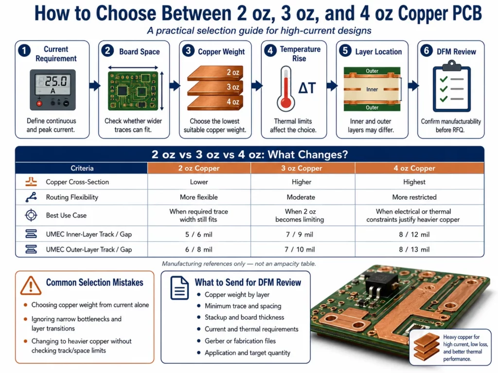
Why Heavier Copper Can Force a Layout Change
A common late-stage problem occurs when you increase copper weight after most of the layout is complete. The new copper specification may no longer fit the original track and spacing assumptions.
This can affect narrow routes near components, crowded inner layers, transition areas, and other locations with little geometric margin. The risk grows when the design team selects copper solely from electrical calculations while the sourcing team treats copper weight as a fabrication note that can be changed later.
The preventive step is to compare the selected copper weight with the supplier’s actual DFM limits before releasing the Gerber files. If the layout does not fit, it is usually better to adjust routing deliberately at the design stage than to discover the conflict during quotation or production preparation.
Common Copper-Weight Selection Mistakes That Lead to Redesign
Several recurring mistakes can make a 2 oz vs 3 oz vs 4 oz decision more difficult than it needs to be.
Three Mistakes to Catch Before Gerber Release
The first is choosing copper weight from current alone. Current is an important input, but allowable temperature rise, trace width, layer location, and operating environment also affect the design.
The second is using heavier copper to compensate for a local bottleneck. If a 4 oz conductor becomes narrow at one point, that section can still concentrate resistance and heat.
The third is choosing copper before checking manufacturing geometry. UMEC’s 2 oz, 3 oz, and 4 oz track/gap values are not identical, so a layout that fits one copper weight may require changes at another.
A practical rule is to avoid freezing the copper specification until you review the electrical requirements and manufacturable geometry together.
What Should Buyers Confirm Before Ordering a 2 oz, 3 oz, or 4 oz PCB?
By the RFQ stage, copper weight should be part of a complete manufacturing specification, not an isolated request.
Useful information includes copper weight by layer, stackup, minimum trace and spacing, relevant continuous and peak-current conditions, operating environment, finished board requirements, fabrication files, application, and target quantity. The exact information required may vary with the project, but the supplier needs enough detail to evaluate the real layout rather than quote an abstract “3 oz PCB.”
What to Include in a Copper-Weight DFM or RFQ Package
The fabrication package should make the layer-specific copper requirement unambiguous. If inner and outer layers differ, state both. If there are unusually narrow areas in high-current paths, they must be visible in the supplied design files rather than represented only by a nominal copper weight.
The objective is to let design, sourcing, and manufacturing evaluate the same board. This reduces the risk of selecting a copper weight that meets an electrical goal but requires an unexpected layout change.
How to Evaluate a PCB Supplier for 2 oz, 3 oz, and 4 oz Designs
A suitable supplier needs to provide more than a statement that heavy copper is available. Buyers need to look for copper-weight-specific inner- and outer-layer track/space information, stackup review capability, and a process for identifying manufacturability conflicts before production.
SZ UMEC CO., LTD publishes Heavy Copper PCB capability data by copper weight, including separate inner- and outer-layer values for 2 oz, 3 oz, and 4 oz. This lets engineers and procurement teams compare the intended design with published fabrication limits before requesting a quote.
Conclusion
The right choice between 2 oz, 3 oz, and 4 oz copper is the lowest copper weight that satisfies the electrical and thermal requirements while remaining practical to route and manufacture. Start with current and temperature constraints, check whether wider traces can solve the problem, then evaluate heavier copper only when the design needs it.
Before releasing the board, compare the selected copper weight with layer-specific track/space limits and review the complete stackup. For a sourcing or DFM review, contact UMEC with the relevant PCB files, copper requirements by layer, stackup, minimum trace/space, operating conditions, application, and target quantity. These inputs provide a clearer basis for evaluating manufacturability than copper weight alone.
2 oz vs 3 oz vs 4 oz Copper PCB FAQs
Is 2 oz copper enough for a high-current PCB?
It can be, depending on the required current, trace width, temperature rise, layer position, and operating environment. If a practical 2 oz trace geometry meets the electrical and thermal target, there may be no need to move to 3 oz or 4 oz.
When should I move from 2 oz to 3 oz copper?
Consider 3 oz when a 2 oz design requires impractically wide power traces, cannot meet the required electrical or thermal target, or creates unacceptable layout constraints. Confirm the corresponding track/space capability before changing the specification.
When do I need a 4 oz copper PCB?
A 4 oz PCB is more appropriate when the project has a defined current-density, space, resistance, or thermal constraint that 2 oz or 3 oz cannot satisfy efficiently. Don’t select it solely for extra safety margin, because heavier copper may require larger track and spacing rules.
Does thicker PCB copper require wider trace spacing?
It often changes the fabrication window. For example, UMEC publishes larger inner- and outer-layer track/gap values for 4 oz copper than for 2 oz copper. Check the exact requirement against the selected PCB manufacturer’s capabilities.
Should I use heavier copper or wider PCB traces?
If you have enough routing area, widening traces is usually the first option. Heavier copper matters more when board space is limited, or when you can’t meet electrical and thermal targets with a practical trace width.