
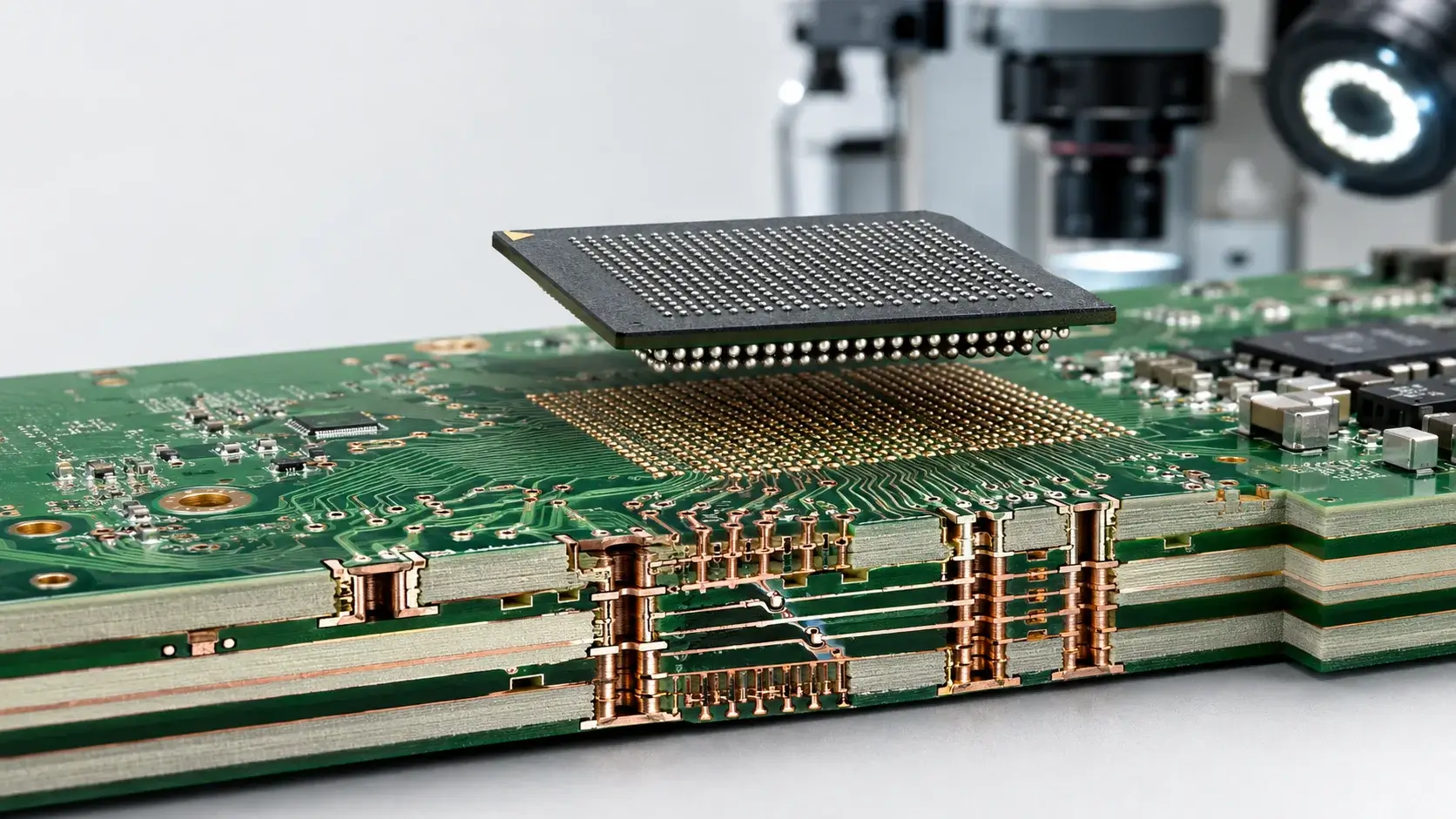
A 0.4mm BGA fanout is rarely a simple routing task. At this pitch, the available space between pads is so limited that standard dog-bone fanout, ordinary through-hole vias, and late-stage stackup changes can quickly lead to manufacturing holds, soldering defects, or expensive board respins. For engineers and procurement teams working on compact electronics, the real question is not only “Can this BGA be routed?” but “Can it be fabricated, assembled, inspected, and repeated reliably?”
This guide explains how to judge whether an HDI PCB design needs via-in-pad, laser microvias, filled and capped vias, or a more advanced stackup. It also covers what to confirm with an HDI PCB manufacturer such as UMEC before sending a 0.4mm BGA PCB design for a quotation.
Quick Answer: Does a 0.4mm BGA Require HDI?
For most 0.4mm pitch BGA designs, HDI technology is required or strongly recommended. A standard multilayer PCB may work for larger BGA pitches. Still, at 0.4mm, the routing channel between pads is usually too narrow for conventional dog-bone fanout with mechanically drilled vias.
The decision depends on the BGA pin count, pad diameter, available routing layers, trace/space capability, signal speed, and assembly requirements. If inner rows cannot escape without violating clearance rules, the design usually needs via-in-pad microvias, blind vias, buried vias, or an HDI stackup such as 1+N+1, 2+N+2, or Any-Layer HDI.
When Standard Dog-Bone Fanout Stops Working
Dog-bone fanout places a via outside the BGA pad and connects it with a short trace. This can be practical for coarser pitches such as 0.8mm or some 0.65mm packages. At 0.4mm pitch, however, pad-to-pad clearance may leave little or no room for a manufacturable trace, annular ring, solder mask dam, and spacing to adjacent copper.
The warning signs are clear: the layout requires trace widths below the fabricator’s normal capability, the solder mask web becomes too narrow, or inner BGA rows cannot escape without cutting planes or creating return-path issues. In that case, forcing a dog-bone strategy usually increases risk rather than reducing cost. The next step is to request a DFM review from the PCB supplier before completing the layout.
Why Via-in-Pad and Microvias Become the Practical Route
Via-in-pad places the via directly inside the BGA pad, allowing inner-row signals to drop into adjacent layers without consuming surface routing channels. For fine-pitch BGA PCB design, this often makes the difference between a board that is theoretically routed and a board that can actually be produced.
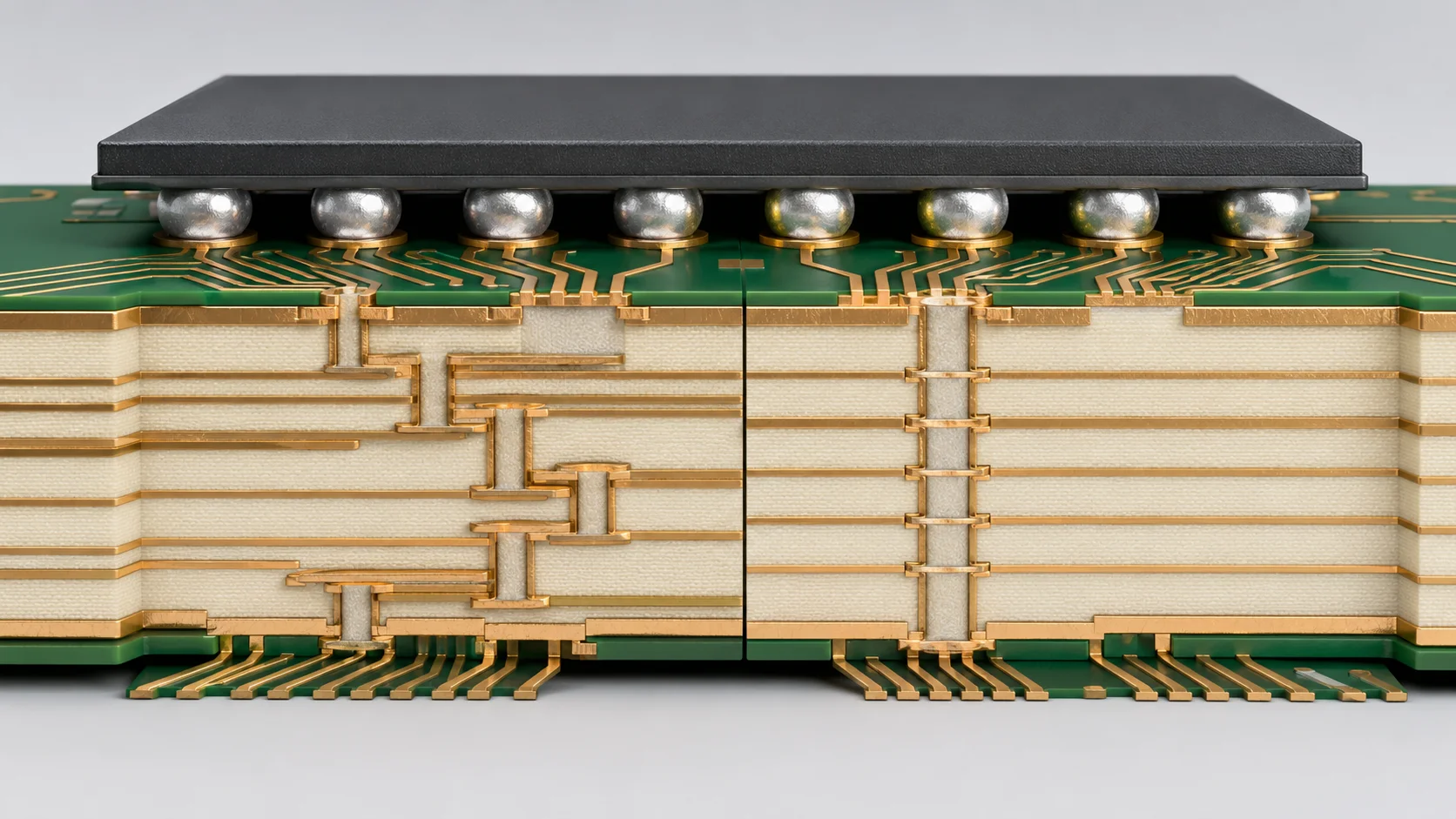
Microvias are especially useful because they are laser drilled and typically connect adjacent layers. This shorter transition can reduce routing congestion and limit via stubs compared with through-hole vias. The tradeoff is manufacturing complexity. Via-in-pad usually requires proper filling, capping, and planarization to prevent solder from wicking into the via during reflow. Before procurement approves a supplier, the via-in-pad process, the minimum laser microvia size, the via fill method, and the inspection plan should be confirmed.
Key Design Constraints Before Routing a 0.4mm BGA
A successful 0.4mm BGA fanout starts before routing. The BGA pitch alone is not enough to define the design rule. Engineers should check the BGA land diameter, solder mask style, trace width and spacing, microvia diameter, capture pad, stackup target, and assembly method as a single, integrated system.
Pad Size, Solder Mask and Routing Channel Limits
At 0.4mm pitch, small changes in pad size can affect the entire fanout plan. A larger pad may increase the solder joint area but reduce routing clearance; UMEC supports a minimum BGA line width and spacing of 2 mils. The typical diameter of laser-guided micro-holes is 0.075-0.1 mm. A smaller pad may open routing space but must still match the component package and assembly process. Solder mask-defined and non-solder mask-defined pads should be selected based on the package recommendation and the fabricator’s capabilities.
Procurement teams should not treat pad size as only a layout detail. It affects yield, assembly quality, and supplier selection. Before releasing files, confirm the manufacturer’s minimum trace/space, solder mask registration, minimum BGA pad capability, and compatibility of the chosen surface finish with fine-pitch assembly.
Manufacturer Capability Limits That Affect First-Pass Success
A 0.4mm BGA design may look acceptable in CAD. Still, it may fail during fabrication review if the selected supplier cannot support the required microvia, line width, spacing, or via-filling process. This is why early DFM matters.
For projects involving fine-pitch BGA routing, buyers should ask for more than a price. Confirm laser drilling capability, via-to-conductor spacing, microvia pad size, controlled impedance tolerance, electrical testing, X-ray inspection for BGA assembly, and whether the supplier can support prototype and later production quantities under the same design rules.
UMEC supports HDI PCB projects involving micro-blind/buried vias, fine-pitch traces, controlled impedance, and BGA assembly review through its HDI PCB manufacturing capabilities page.
Via-in-Pad and Microvia Choices for 0.4mm BGA Fanout
The via structure drives routing density, cost, reliability, and manufacturability. For 0.4mm BGA escape routing, the best option is usually not the cheapest via. It is the via structure that matches the pitch, layer transition, assembly process, and reliability requirement.
Through-Hole, Blind, Buried and Laser Microvias: Which One Fits?
Through-hole vias pass through the entire PCB and can create routing blockages under dense BGAs. They may also leave unused via stubs, which can matter in high-speed designs. Blind vias connect an outer layer to an inner layer, buried vias connect internal layers, and laser microvias are commonly used for short HDI transitions.
For 0.4mm BGA designs, laser microvias and via-in-pad are often preferred because they save surface routing space. Blind and buried vias may still be needed depending on the stackup. The wrong choice can increase lamination cycles, create spacing violations, or make the board harder to inspect. A practical next step is to send the proposed stackup and BGA footprint to the PCB manufacturer before final routing.
Filled, Capped and Plated-Over Via-in-Pad Requirements
Via-in-pad for BGA assembly should usually be filled and capped or plated over. If a via remains open in the pad, solder can wick into the hole during reflow, resulting in insufficient solder volume, voids, outgassing, or unreliable joints. This risk becomes more serious at 0.4mm pitch because the solder joint is already small.
When requesting a quote, specify whether via-in-pad holes require resin filling, copper cap plating, or another approved process. The RFQ should also identify which vias are in BGA pads and whether X-ray inspection is required after assembly. This prevents quotation ambiguity and reduces the chance that a supplier will price a simpler process that does not match the design intent.
Stacked vs Staggered Microvias for Reliability and Cost
Stacked microvias allow compact vertical transitions, which can be helpful for dense BGA breakout. However, stacking can increase process sensitivity and may require tighter control of plating, registration, and lamination. Staggered microvias can reduce some reliability concerns but may consume more routing space.
The choice should be based on routing density, number of BGA rows, current and signal requirements, thermal cycling expectations, and cost targets. If the product is used in automotive, medical, aerospace, industrial, or high-reliability environments, microvia reliability should be reviewed early. Ask whether microsection analysis, thermal cycling, or additional reliability testing is appropriate for the application.
HDI Stackup Choices for 0.4mm BGA Designs
Stackup selection is one of the main cost-and-yield decisions in HDI PCB design. It affects fanout, impedance, lamination cycles, assembly behavior, and lead time.
1+N+1, 2+N+2 and Any-Layer: How to Choose
A 1+N+1 stackup may be enough when only one buildup layer is needed on each side, and routing density is moderate. A 2+N+2 stackup adds more routing flexibility for dense BGAs. Any-Layer HDI enables microvia interconnections across multiple layers and may be used when routing freedom is more important than cost control.
| Stackup Type | Routing Flexibility | Cos | Typical Use Case | Lamination Cycles |
| 1+N+1 | Moderate | Low | Simple HDI, moderate density | 1 |
| 2+N+2 | High | Medium | Dense BGA, fine pitch | 2 |
| Any-Layer | Very High | High | Ultra-dense, maximum freedom | Multiple |
For 0.4mm BGA fanout, the right stackup depends on BGA row count, I/O density, signal grouping, power distribution, and whether high-speed signals need controlled impedance. Procurement should confirm lamination cycles and manufacturing limits before approving a stackup, as each additional buildup stage can affect price, lead time, and yield risk.
How Stackup Affects Impedance, Signal Integrity and Assembly Yield
A stackup is not only a mechanical layer plan. It defines dielectric thickness, reference planes, return paths, and impedance behavior. Poor stackup choices can create discontinuities around microvias, split reference planes, or unstable impedance for high-speed interfaces.
For designs with RF, high-speed digital, or dense processor BGAs, controlled impedance should be specified clearly. Material selection may also matter. High-Tg FR-4, halogen-free laminates, low-loss materials, or hybrid stackups should be verified against the signal speed, thermal environment, and cost target. The stackup should be reviewed by fabrication and assembly teams before production release.
Common Failure Risks in 0.4mm BGA HDI Boards
Fine-pitch BGA failures often stem from small design and process mismatches rather than a single obvious mistake. The most common risks involve via-in-pad preparation, solder behavior, microvia reliability, and incomplete DFM communication.
Solder Wicking, Voiding and Outgassing from Improper Via-in-Pad
If via-in-pad holes are not properly filled and capped, solder may drain away from the BGA joint during assembly. This can cause opens, weak joints, voids, or inconsistent solder volume. Outgassing can also disturb the solder joint during reflow.
The prevention method is straightforward: define the via-fill and cap requirements in the fabrication notes, confirm the surface finish, and request inspection steps appropriate to the risk level. For BGA assembly, X-ray inspection is often used because hidden solder joints cannot be judged visually.
Microvia Plating and Thermal Cycling Risks
Microvias are small, but they carry real mechanical and electrical responsibility. Plating quality, aspect ratio, material CTE, stacked structures, and thermal cycling can all affect long-term reliability. A design that passes initial electrical testing may still need closer review if it will operate under temperature swings, vibration, or high current density.
Risk can be reduced by avoiding unnecessary stacked microvias, using approved aspect ratios, selecting suitable materials, and reviewing the design with the fabricator before release. For higher-reliability applications, additional inspection such as microsection analysis or thermal testing may be appropriate.
DFM and RFQ Checklist Before Sending a 0.4mm BGA HDI PCB for Quote
A strong RFQ shortens the path from design review to usable quotation. It also helps avoid a common problem: receiving a low initial price that changes after DFM questions reveal missing details.
Files and Specifications Your PCB Supplier Needs
For a BGA HDI PCB quote, the following information is required.
- Drill files
- Stackup requirements
- BGA pitch information
- Via-in-pad notes
- Impedance requirements
- Material preference
- Surface finish
- Spessore della scheda
- Copper weight
- Quantity and target lead time
If the project is still in layout, send the BGA footprint, proposed stackup, and routing constraints for early review. Early feedback is usually less expensive than redesigning after fabrication hold.
Questions to Ask Before Choosing an HDI PCB Supplier
Before selecting a supplier, ask whether the factory can support the required laser microvia size, minimum trace/space, via filling, BGA pad size, controlled impedance, electrical testing, and BGA X-ray inspection. Also confirm whether prototype rules match production rules, especially if the product may scale from engineering samples to medium-volume manufacturing.
A supplier should be able to review manufacturability, explain stackup tradeoffs, and identify design risks before production begins. This is especially important for teams balancing compact size, schedule pressure, and high assembly yield.
UMEC HDI PCB Capabilities for Fine-Pitch BGA Projects
Selecting an HDI PCB supplier for 0.4mm BGA work is partly a technical decision and partly a communication decision. The supplier should understand microvia structures, fine-line routing, via-in-pad processing, controlled impedance, and assembly inspection. It should also provide practical feedback before the design is locked.
UMEC offers PCB fabrication, PCB design support, component sourcing, PCB assembly, and testing services for projects that need a connected manufacturing path from prototype to production. For HDI PCBs, confirmed capabilities include HDI buildup structures, laser microvias down to 0.075mm in advanced capability, fine line/space support, controlled impedance capability, and BGA assembly support with X-ray inspection.
For teams that need more than bare-board fabrication, More Than PCB offers a broader one-stop manufacturing approach, including design, fabrication, components, assembly, and testing support. Engineers and buyers can also start from UMEC to review the wider service scope.
Conclusion
A 0.4mm BGA fanout should be planned as an HDI manufacturing decision, not only a PCB layout task. The safest path is to define the BGA pad strategy, via-in-pad process, microvia structure, stackup, impedance requirements, and inspection plan before routing is finalized.
For procurement teams, the most useful RFQ is the specific one. Include the BGA pitch, stackup target, material requirements, via-filling notes, impedance requirements, assembly files, inspection expectations, quantity, and application environment. When these details are ready, contatto UMEC to request a DFM review or quotation for an HDI PCB project involving fine-pitch BGA routing.
FAQs
Can a 0.4mm BGA be routed without HDI?
Sometimes, but it is uncommon for dense 0.4mm BGA designs. If the BGA has few pins and enough routing channels, a simpler structure may work. For most compact layouts, HDI PCB fanout with microvias or via-in-pad is needed.
Is via-in-pad required for every 0.4mm BGA ball?
Not always. Outer rows may route directly on the surface or use other escape methods. Inner rows often need via-in-pad microvias. The final decision depends on pin count, routing density, stackup, and manufacturer capability.
Should microvias be stacked or staggered for 0.4mm BGA fanout?
Stacked microvias save space and enable denser routing, but they may increase process sensitivity. Staggered microvias can be more forgiving in some designs but need more layout area. The choice should be reviewed through DFM before production.
What should be checked before ordering a 0.4mm BGA HDI PCB?
Check BGA pad size, trace/space, laser microvia size, via fill and cap requirements, HDI stackup, controlled impedance, material selection, surface finish, electrical testing, and X-ray inspection requirements.
What files are needed for a 0.4mm BGA PCB fabrication quote?
Provide Gerber or ODB++ files, drill files, stackup, via-in-pad notes, impedance requirements, material and surface finish preferences, board quantity, and lead-time target. For assembly, include BOM, Centroid data, and assembly drawings.