

A complete flex PCB prototype checklist gives a manufacturer enough information to price the same construction you intend to build. Before sending Gerber files, define the flex circuit’s use, stackup, materials, geometry, bend conditions, finishes, and acceptance data. Skip one critical item, and the estimator may pause for clarification. Missing specifications also push cost, lead time, and reliability away from your plan.
The twelve items below form a practical RFQ package for engineering and procurement teams. Record each requirement in the fabrication drawing or an approved stackup, not only in email. Where a value is still open, label it for manufacturer review. That way, every quotation rests on a visible decision rather than an unstated default. This checklist covers what goes into an RFQ before you request a quote; supplier qualification and design-for-manufacture review come later.
The 12 Specifications to Put in Your RFQ
| Specification | What to Send | Typical Format |
| Application and Bend Use | One-time install bend or repeated motion, bend angle, cycle count, operating temperature | Fabrication drawing note, bend table |
| Layer Count and Stackup | Every conductive, dielectric, adhesive, coverlay, shield, and stiffener layer in order with nominal and finished thickness | Stackup table, lamination drawing |
| Base Film and Adhesive Construction | Base-laminate adhesive construction, film thickness, plus coverlay, bondply, and stiffener adhesive layers | Material callout, datasheet reference |
| Copper Type and Copper Weight | Foil type, starting weight, and whether limits assume base or finished copper | Fabrication drawing note |
| Finished Thickness and Tolerances | Overall target, local targets at connectors and stiffeners, and measurement locations | Fabrication drawing, thickness table |
| Trace Width, Spacing, and Copper Clearances | Minimum width and spacing by copper weight, plus copper-to-edge, copper-to-hole, and copper-to-bend values | Gerber layers, DFM summary |
| Holes, Vias, and Annular Rings | Separate drill data for plated, nonplated, slots, and laser features with finished diameters and pad sizes | Drill file, drill chart |
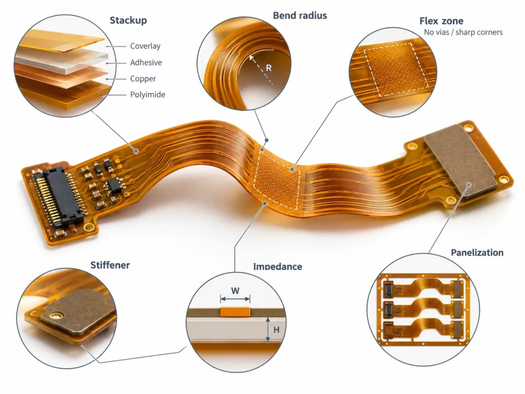
| Bend Radius and Flex-Zone Restrictions | Inside radius per bend, bend direction, static or dynamic use, and prohibited features in the bend | Fabrication drawing, keepout layer |
| Coverlay Openings and Stiffeners | Coverlay opening geometry and pad clearance, plus stiffener material, thickness, adhesive, and outline | Coverlay drawing, stiffener detail |
| Controlled Impedance Requirements | Net or geometry, target impedance, tolerance, reference plane, and test method | Impedance table, stackup cross-section |
| Surface Finish, Panelization, and Delivery Format | Finish type and its driver, plus array size, rails, tooling holes, fiducials, and delivery format | Panel drawing, assembly drawing |
| Complete Manufacturing Data and Revision Control | Synchronized fabrication data, netlist, drawings, tables, and one revision identifier | Release package, readme file |
Application and Bend Use
State what the flex circuit does and where it fits. Say whether it bends once during installation or moves repeatedly in service. For dynamic use, add the expected motion, bend angle, cycle requirement, and operating temperature. A frequent cause of rework is a drawing that shows a circuit “dynamic” without stating the bend angle or the cycle count. Those two numbers drive conductor direction, neutral-axis placement, and flex-zone keepouts more than any other input, and a target the drawing never states is a target the estimator has to invent before any price can be issued. This context lets the manufacturer review copper type and flex-zone risks against the real mechanical duty. It also lets the estimator price the bend a 2 million cycle target implies. Classify one-time installation as static and repeated motion as dynamic before you send the file, then ask UMEC to confirm the classification in writing against the cycle target. Drop the wrong label and the review shifts with it. These are planning references, not a specification.
Layer Count and Stackup
Show every conductive, dielectric, adhesive, coverlay, shielding, and stiffener layer in order, including nominal and finished thicknesses plus tolerances. Each layer contributes its own thickness and bond line. A three-layer flexible PCB does not carry the same thickness budget as a single-sided one. A common omission in first-pass RFQ packages is the bond line between the coverlay and outer copper, which quietly changes the finished thickness the connector has to accept. A 25 um gap there is enough to fail a connector fit check. Identify plated and unplated features and any local thickness change. A defined flex PCB stackup prevents two suppliers from quoting different constructions under one layer count. It also exposes lamination or registration issues before tooling. Reviewers reject the package—planning reference only; not a released manufacturing specification.
Base Film and Adhesive Construction
Name the flexible dielectric family and its thickness. State whether the copper-clad base laminate is adhesive-based or adhesiveless, then identify the coverlay adhesive, bondply, and stiffener adhesive separately where they apply. Polyimide base film is commonly supplied from 12.5 um to 50 um, with coverlay adding roughly 25 um to 50 um per side. The adhesive layer runs 12 to 25 um. If material selection is still open, provide thermal, dimensional, flammability, and assembly constraints instead of naming an arbitrary grade, and ask UMEC to return the proposed film and adhesive system for your approval. A common gap is a drawing that lists base film thickness but leaves the adhesive system unstated, so two suppliers quote the same film with different bonds and the difference only surfaces at incoming inspection. Material availability and bonding method change thickness, flexibility, and processing schedule. Use this value for early screening, then obtain project-specific approval.
Copper Type and Copper Weight
Call out the copper foil type and starting weight. Note the finished copper expectation and any plating requirement. Rolled-annealed copper suits repeated bending far better than electrodeposited foil, and that difference decides the bend life of a dynamic circuit. Rolled-annealed material is typically available from about one third of an ounce up to 2 oz. One ounce of copper is roughly 35 um thick. Heavier copper changes etching capability and the minimum geometry a shop can hold, so confirm the copper choice for the bend duty. A frequent surprise is a drawing that calls for rolled-annealed foil at 2 oz in a tight flex zone. The raised etch factor shrinks the achievable line width, and the layout that passed review at 1 oz no longer fits the same area. These are planning references, not a specification.
Finished Thickness and Tolerances
Give the target thickness for the overall circuit and for critical connector or reinforced areas. Add tolerances only where the assembly needs them. Identify thickness measurement locations, because coverlay, adhesive flow, copper plating, and stiffeners all create local variation. A single-sided flexible PCB might sit near 100 um at the flex zone. It reads far thicker where a stiffener is bonded behind a connector. The drawing has to say which number applies where. Excessively tight blanket tolerances raise review time and price. A common argument starter is a note that gives one blanket plus or minus 5% to 10% tolerance without naming the flex zone or the stiffened area. Confirm this range against the final stackup and the fabricator’s process.
Trace Width, Spacing, and Copper Clearances
List minimum trace width and spacing by copper weight. For routine flexible constructions, a 50/50 um width and spacing pair is a workable starting point. Tighter geometry needs a higher density process. Then define copper-to-edge, copper-to-hole, and copper-to-bend clearances. Mark neck-downs or dense regions instead of relying on one global minimum. These relationships help the supplier evaluate etch compensation, registration allowance, and yield. One frequent mismatch is a drawing that quotes the finest line width next to a heavy copper callout. The etch process cannot hold that pairing, and the shop has to either widen the trace or change the copper before it can quote—planning reference only; not a released manufacturing specification.
Holes, Vias, and Annular Rings
Provide separate drill data for plated holes, nonplated holes, slots, and laser features. Specify finished diameters, tolerances, via treatment, and pad sizes. Add annular-ring expectations. Keep vias at least 0.5 mm clear of every bend line unless the construction has been specifically reviewed. A via placed in a moving zone concentrates stress at the barrel and shortens life. A drill file without these notes leaves open questions about plating and hole ownership. It also hides whether the pad geometry can absorb registration movement. A common ambiguity occurs when a slot and a plated hole share one drill table with no ownership column, so the shop cannot tell which features receive copper and which must stay bare. Right there, the quote stops. Subject to design review; do not treat this as a released specification.
Bend Radius and Flex-Zone Restrictions
Dimension each bend zone and state the required inside radius. A common rule of thumb calls for at least 6 times the total thickness for a single-copper static bend. It requires 12 times the thickness for a double-copper static bend and 24 times for a multilayer static bend. Dynamic bends need far more room: 100 times the thickness for one layer, 150 times for two. Show prohibited features such as vias, component pads, and sharp copper corners. State the bend direction and whether the bend is static or dynamic. The acceptable radius depends on thickness, layers, materials, copper, and motion. Request a design-specific review from UMEC rather than treating one rule of thumb as universal. A frequent defect is a design built to the static radius that is then cycled in service. The copper cracks long before the prototype reaches production.IPC-2223E organizes bend requirements by installation use, so cite the revision that fits the duty you described. These are planning references, not a specification.
Coverlay Openings and Stiffeners
Define coverlay material, opening geometry, registration tolerance, and clearance around pads. For every stiffener, identify material, thickness, adhesive, outline, and finished thickness at the interface. Allow at least 0.5 mm from the stiffener edge to the start of the bend. That 0.5 mm margin keeps the rigid support from pinching the flex zone. Include connector contact requirements and the transition from rigid support to the bend area, and ask UMEC to return the stiffener outline with the finished thickness at that interface marked. One very common revision comes from a stiffener outline drawn flush to the bend line, so the board is handled flat in assembly and then cracks at the stiffener edge on the very first pass. These details prevent squeeze-out, misregistration, and stress concentration from becoming late drawing changes. Confirm this range against the final stackup and the fabricator’s process.
Controlled Impedance Requirements
For impedance-controlled circuits, identify each net or geometry, target impedance, tolerance, reference plane, and test requirement. Impedance targets are commonly held to plus or minus 5% to 10%, depending on the stackup and the process. Supply the intended stackup. Alternatively, allow the fabricator to return a proposed one. Confirm whether coupons and time-domain reflectometry reports are required. Coverlay, dielectric thickness, copper profile, and process tolerance all affect the model. That matters most where a trace crosses different flex constructions. Impedance often misses at the transition between a stiffened region and the flex zone. There, the dielectric environment, conductor spacing, or reference structure may change, and the trace width may not be adjusted to match. A flexible PCB makes that transition harder to control than a rigid board. Use this value for early screening, then obtain project-specific approval.
Surface Finish, Panelization, and Delivery Format
Name the surface finish and any connector, soldering, wire-bonding, or storage constraint that drives it. Add array dimensions, rails, tooling holes, fiducials, routing method, and permitted breakaway features. State whether parts must arrive individually, in panels, or on an assembly carrier. A panel that packs more parts per sheet can lower unit material use, yet it may also weaken handling for thin flexible circuits and shift parts before the finish is applied. That trade-off belongs on the drawing, not in a later email. A frequent issue is a 3 mm rail width chosen for a rigid panel. Under a thin flexible PCB, that rail flexes too much. These are planning references, not a specification.
Complete Manufacturing Data and Revision Control
Release synchronized Gerber or ODB++ data, drill files, netlist, fabrication drawing, stackup, impedance table, panel drawing, readme, and a single revision identifier. Remove obsolete layers and resolve conflicts between notes and data. Align the release package with IPC-6013 acceptance requirements so inspection criteria follow the same document the shop builds from. A pre-release DFM review or PCB design and layout service can close gaps before an estimator turns uncertain inputs into quote assumptions. The most common source of confusion is a folder that holds two drawing files with different revision letters alongside one Gerber set, so the estimator has to stop and ask which revision is current. Do not let that guess reach the quote. Ask UMEC to confirm the revision it priced before you release the order. Subject to design review; do not treat this as a released specification.
Build a Quote-Ready Flex PCB Prototype Package
Send a short RFQ cover sheet with quantity breaks, target schedule, prototype purpose, assembly responsibility, test expectations, and any approved alternates. One page is enough. It lets the estimator separate a real requirement from a preference before the package reaches engineering.
Use a supplier’s published limits as a screening tool, then request confirmation for the complete feature combination. A single capability number rarely survives contact with a real design. UMEC’s flex PCB manufacturing capability table lists the process envelope for flexible and rigid-flex work. IPC-2223 sets the sectional design framework for flexible boards. Compare both against your drawing before you treat any value as settled.
The commercial package should also name the inspection records you need. Review UMEC’s quality assurance process, then confirm the applicable incoming, in-process, and final inspection criteria in the RFQ itself. IPC-6013 defines the qualification and performance requirements for flexible printed boards, so cite the project-specified revision, the performance class, the construction type, the installation and usage classification, and any AABUS items. For repeated flexing, also state the cycle count, bend radius, and bend angle. Name the revision, and you remove one more clarification round.
Conclusion
A useful flex PCB prototype checklist removes ambiguity before you commit to price and schedule. Define all twelve specifications and align the drawing with the data package. Confirm the manufacturing envelope against IPC-2223 design limits and IPC-6013 acceptance criteria. Small omissions create large quotation errors. That is why the checklist matters more than the quote itself.
Frequently Asked Questions
Can I Request a Flex PCB Quote With Gerber Files Only?
Gerbers may support a preliminary estimate, but they rarely define materials, bend use, stackup tolerances, stiffeners, impedance, panelization, or acceptance data. Those inputs drive both cost and buildability. Send the fabrication drawing and stackup with the data set. Treat a Gerber-only quote as a placeholder, not a commitment.
Which Specification Causes the Most Quote Delays?
No single item causes every delay, but an undefined stackup often affects several decisions at once. Materials, finished thickness, bend radius, impedance, and panelization all follow from it. Fix the stackup first. The remaining specifications then have a frame to sit in, and the estimator can price the rest without guessing.
How Should I Specify Bend Radius for a Prototype?
State the required inside radius, bend angle, bend direction, available envelope, and static or dynamic use. For moving circuits, include the cycle and temperature target. A static-only description on a part that cycles in service is the most expensive omission on the list. If in doubt, mark it dynamic and let the manufacturer confirm.
Should the Prototype Use the Same Stackup as Production?
Use the intended production construction whenever the prototype must validate bend behavior, impedance, connector fit, or assembly handling. If a substitute is unavoidable, document how it differs. A prototype that proves the wrong build teaches nothing. Confirm which deviations are acceptable before the order is placed.
Request a Prototype Fit Check
For a fit check, send UMEC’s technical team the synchronized manufacturing package, quantity, application, bend conditions, target schedule, and required documentation. Include the open questions. A short list of unknowns is more useful than a complete drawing that hides them.