
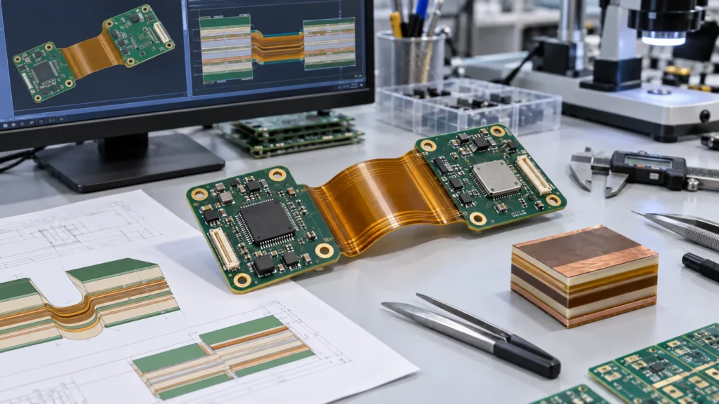
A rigid-flex PCB stackup is not simply a rigid multilayer with a flexible tail. It is a single mechanical and electrical system in which the rigid regions, flex regions, and transitions may require different layer constructions. The stack must support component density and microvias in the rigid areas, predictable return paths for controlled impedance, and a flex thickness that can bend without concentrating strain in copper or plated features.
Build the stackup before detailed routing. Start with the product’s folding or motion requirement, define the materials and zones, then add HDI and impedance features without making the bend section unnecessarily thick. Review the final construction with the fabricator because dielectric availability, copper type, drilling sequence, registration, and lamination flow determine whether the proposed geometry is repeatable.
Six Steps to a Released Rigid-Flex PCB Stackup
- Define the bend duty and fold sequence. Record direction, angle, available radius, cycle count, and installation order before any layer decision.
- Draw the zone map. Mark rigid islands, flex spans, transition boundaries, stiffeners, bend lines, and keepouts.
- Select the flex material system. Choose FCCL type, copper type and weight, coverlay, adhesive or bondply, and shielding as one set.
- Set the layer count and specify which layers continue into the flex. Continue only those that must cross the bend.
- Add HDI features in the rigid region only where escape density requires them. Keep microvias clear of bend and transition zones.
- Recalculate impedance per zone and release the package for the fabricator’s DFM review. Freeze the stackup revision before routing.
What the Stackup Must Resolve
A usable stackup answers three questions: density, where the reference paths run, and where the board bends. IPC design standards cover each: IPC-2223 for flexible boards, IPC-2226 for HDI, and IPC-2141 for controlled impedance. Check each value against the material set and the process.
Map Rigid, Flex, and Transition Zones
Classify Every Bend Before Drawing the Outline
Draw the zone map before you pick layer counts. Mark every rigid island, flex span, transition, stiffener, connector, keepout, and bend line. Then classify each bend: installation-only, occasional, or dynamic. Record direction, angle, radius, cycles, and twist.
Keepouts Around the Transition
The zone map surfaces conflicts early: a fine-pitch device pushes microvias toward the transition while the enclosure pulls the bend there. Catch it before routing.
How the Three Zones Differ in Construction
The rigid-to-flex transition starts most construction disputes, so it needs its own column, not an edge of the rigid region.
| Parameter | Rigid region | Flex region | Rigid-to-flex transition |
| Layer count | Full build | Continuing layers (2 typical) | Tapered |
| Base dielectric | FR-4 core + prepreg; high-Tg if required | Adhesive-less polyimide FCCL | No-flow prepreg or bondply |
| Copper type and weight | ED or RA, 1 oz typical | RA copper, 1/2 oz to 1 oz | Matches adjacent layer |
| Outer protection | Solder mask | PI coverlay with adhesive | Coverlay boundary + rigid opening |
| Plated features | Through, blind, buried, microvias | None inside active bend | Teardrops and anchor pads only |
| Primary control | Escape density, plane continuity, impedance | Finished thickness and bend radius | Resin flow, stiffener edge, strain path |
| Common failure mode | Inconsistent reference planes under impedance nets | Extra layers or shielding push radius past enclosure | Sharp outline corners and stiffener edges as stress raisers |
Most bend failures come from something hard inside the bend, not the radius number. Check the last row against your own drawing.
Choose the Flex Material System Before Adding HDI
Select the Flex Material System as One Set
Pick the flexible laminate, copper weight, coverlay, adhesive or bondply, and shielding as one set. Thicker copper, planes, and adhesive add flex thickness and cut bend capability. UMEC’s rigid-flex manufacturing capabilities cover adhesiveless FCCL, coverlay systems, laser drilling, HDI-type structures, and controlled-impedance options. The stack needs approval before routing.
Adhesiveless is the usual start for a thin flex. DuPont’s published Pyralux AC data lists 12 um to 50 um thicknesses, with rolled-annealed and electrodeposited copper at equal weights. That makes copper type a free choice, not a thickness penalty.
Specify copper type, not just weight. Rolled-annealed foil takes repeated bending, and it costs less than reworking a cracked flex after tooling. Electrodeposited foil belongs in rigid sections and static flex-to-install builds. Adhesiveless constructions bond polyimide straight to copper, dodging the acrylic layer’s higher dielectric loss and Z-axis expansion. Adhesive-based systems suit static folds. On the flex, skip solder mask: it cracks at the bend, and coverlay does not. Choose both with the laminate.
Limit What Continues Into the Flex Span
Keep flex conductor and reference layers to the minimum required to support routing, shielding, current, and signal consistency. Bend radius is based on the finished flex thickness, coverlay, and any extra layers, not the bare polyimide core or a single multiplier. Confirm against the actual material and duty cycle.
Adhesiveless FCCL vs Adhesive-Based Constructions
Typical published values for commercial materials, as a planning reference. Confirm Dk, Df, and elongation against the laminate datasheet before any impedance or bend calculation.
| Property | Adhesiveless FCCL | Adhesive-based FCCL | |||
| Bonding layer | Polyimide cast directly onto copper | Acrylic adhesive, approx. 12.5 um to 25 um | |||
| Typical Dk at 1 GHz | approx. 3.4 | approx. 3.6 to 3.8 | |||
| Typical Df at 1 GHz | approx. 0.002 for low-loss grades | Above approx. 0.02 at multi-GHz | |||
| Thermal behavior | Stable through lead-free reflow | Adhesive Tg around 100 C, high Z-axis expansion | |||
| Preferred for | Dynamic bend, high-speed, repeated reflow | Static bend, cost-sensitive builds | |||
| Copper type | Grain structure | Typical elongation at break | Typical use | ||
| Rolled-annealed (RA) | Lamellar | approx. 20% to 40% | Dynamic flex and most flex regions | ||
| Electrodeposited (ED) | Columnar | Lower, often cited near 5% | Rigid regions and static flex | ||
Example Rigid-Flex PCB Stackups by Layer Count
Two questions matter. What does a four-layer build contain, and what changes at six? Both carry one two-layer flex bridge, so bend radius barely moves. Six layers add rigid-region escape, cost more, and do not improve bend. Treat the values as a planning reference, not a specification.
| Item | 4-layer rigid-flex pcb (example) | 6-layer rigid-flex pcb (example) |
| Conductor layers per rigid section | 2 | 4 |
| Layers continuing into the flex span | 2 (one 2-layer flex core) | 2 typical; 4 only after review |
| Flex core | Adhesiveless PI, 25 um or 50 um | Adhesiveless PI, 25 um preferred |
| Flex copper | 1/2 oz or 1 oz RA copper | 1/2 oz RA copper preferred |
| Outer protection in flex | PI coverlay, 25 µm per side | PI coverlay, 25 µm per side |
| Worked finished flex thickness | approx. 0.15 mm to 0.20 mm | approx. 0.15 mm to 0.20 mm with 2 continuing layers; approx. 0.25 mm to 0.35 mm with 4 |
| Typical bend duty | Static fold-to-install | Static; dynamic only after review |
| Relative cost and lead time | Baseline | Higher (additional lamination cycles) |
Four-layer rigid-flex construction (example)
These are common commercial ranges. Treat them as an example, not a specification. Buildability depends on the material system, copper type, lamination sequence, and the fabricator’s process.
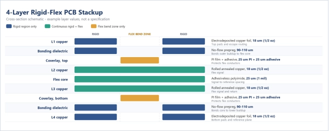
Finished flex thickness works out to about 160 um: 25 um core, 36 um copper, 100 um coverlay.
Six-layer rigid-flex construction (example)
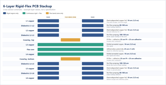
The flex spine fits the four-layer build, so bend radius does not move. Lamination count, registration, and unit cost do.
4 Layer Rigid-Flex PCB: One Flex Core Between Two Rigid Pairs
A 4-layer rigid-flex pcb is where most people start: two conductor layers in each rigid section, a two-layer flex core between them that carries both through. The bend stays thin, so the radius stays small. If the rigid region runs out of escape room, add rigid layers, not flex layers.
6 Layer Rigid-Flex PCB: Four Rigid Layers With a Two-Layer Flex Bridge
In a 6-layer rigid-flex pcb, each rigid section holds four conductor layers. Only two continue across the flex span. Every layer you add to the flex bridge raises thickness and bend radius, so a span that needs two nets bends worse at six and costs more.
Choosing Between 4, 6, and Higher Layer Counts
Justify the move from four layers to a 6-layer rigid flex pcb with the rigid region, never the flex span. Let escape channels and plane pairs set the rigid layer count. An advanced rigid flex HDI PCB built as 1+n+1 or 2+n+2 follows escape density and via relief, not layer count.
Add HDI In Density Actually Requires It
Its rigid region defines an advanced rigid flex HDI PCB. Microvia buildup, blind and buried vias, and sequential lamination add escape density under fine-pitch devices. The flex span stays as thin as the continuing nets allow, so the HDI structure stops at the rigid-to-flex boundary. Use it only where escape or routing density requires. Define which layers each via connects.
IPC-2226 defines microvia and buildup structures, and fabricators quote their via definitions and aspect-ratio limits. Those limits suit rigid constructions. Once a flex core enters the lamination sequence, treat it as a ceiling, not a target.
Buildup Sequence and Lamination Order
A 2+n+2 arrangement places two sequential buildup layers on each side of a core that carries the flex spine. Where the flex core sits matters. Each lamination pass exposes the polyimide and adhesive system to additional heat and pressure and adds registration error at the coverlay edges.
UMEC describes multilayer rigid-flex structures with buried or blind microvias and up to a 2+n+2 HDI arrangement, subject to project review. Check microvia aspect ratio, capture-pad geometry, copper filling, registration, and how sequential lamination meets the rigid-flex bonding cycle.
Where Microvias Belong in a Rigid-Flex Build
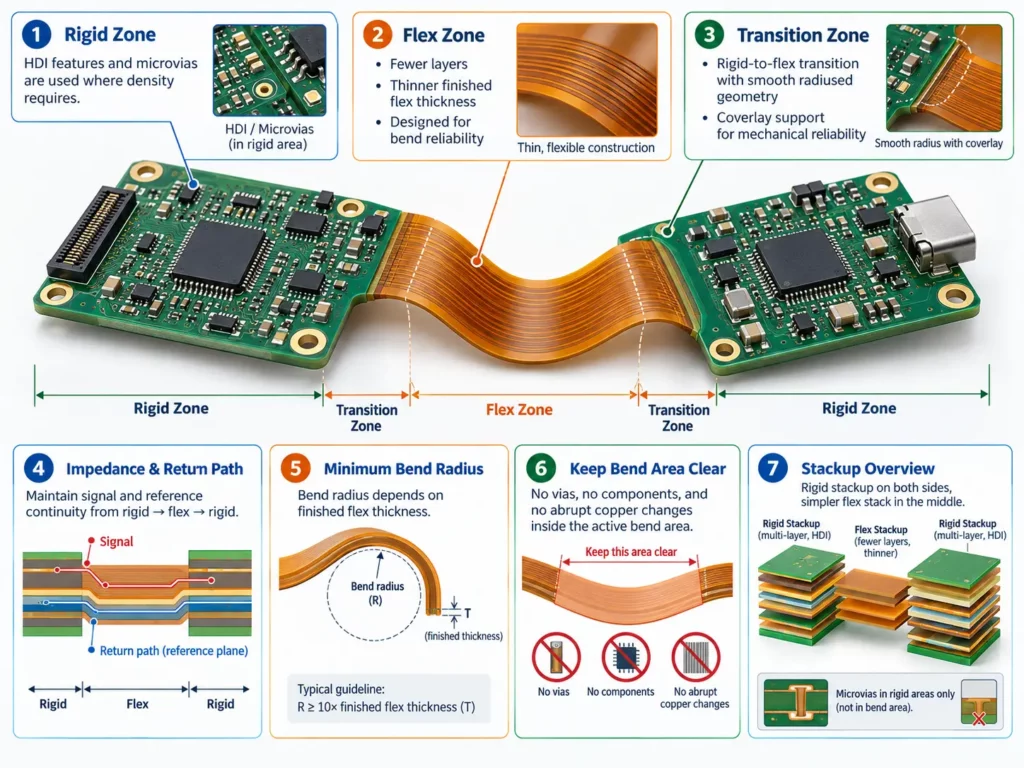
Microvias belong in the rigid islands. A plated microvia is a copper barrel bonded to the dielectric on all sides, with no ductility budget. A dynamic flex allows less strain than a static barrel. Define a keepout spanning the bend line and the transition fillet, and keep rigid plated features, capture pads, filled vias, and copper balancing fill outside it.
Laser-drilled microvias and sequential buildup are standard HDI PCB manufacturing capabilities. In a rigid-flex panel, the practical limit is registration through the flex bonding cycle, not the via itself.
The trade-offs mirror those behind choosing between blind, buried, and microvia structures in a rigid build. Here, every lamination cycle must also survive the bonding step that joins the flex core. So the buildup count lands one lower.
Design Controlled Impedance Across Every Zone
Reference Paths Across Rigid and Flex Zones
A controlled-impedance PCB can use different geometries in rigid and flex sections, but the reference path must be deliberate. For each net class, record the signal layer, reference layer, target impedance, tolerance, dielectric and copper thickness, and transition. Recalculate when a signal enters a thinner flex build. Flex routing favors thin microstrip. A stripline contains the field better but requires another reference layer. Keep return current continuous across layer changes, keep transition vias out of stressed areas, and provide the fabricator with an impedance table tied to the approved stackup revision and a coupon.
Recalculating Trace Geometry for the Flex Section
A 50-ohm single-ended trace over a 100 um rigid dielectric at er near 4.0 comes out about 0.17 mm wide using 18 um copper. Move that same net onto a 50 um polyimide core in the flex span, and the target lands near 0.075 mm. Treat these widths as illustrative, not a process limit.
Protect Bend Reliability in Copper and Coverlay
Sizing Bend Radius From Finished Flex Thickness
Route conductors perpendicular to the bend line, with smooth curves instead of sharp corners. In the active bend, avoid abrupt width changes, neck-downs, pad entries, and stacked copper. When traces share more than one flex layer, stagger them and see whether that lowers aligned strain.
Coverlay, Stiffener, and Outline Details at the Transition
At the rigid-to-flex transition, keep outline radii smooth. Define the coverlay boundary, rigid opening, stiffener edge, and adhesive allowance. Then check how the board meets the enclosure. A flex that looks safe can still be forced over a sharp edge.
See the rigid-flex DFM checks for bend radius.
Close the Stackup With a Fabricator DFM Review
What Belongs in the Release Package
Release one integrated package: zone drawing, approved stackup, rigid and flex thicknesses, material callouts, coverlay and stiffener details, drill and via tables, impedance requirements, bend map, and the assembly fold. UMEC’s PCB design and layout service covers DFM support, Gerber checks, panelization, and signal-integrity work.
Questions to Put in Writing
Connect density, signal reliability, and mechanics in one review, not separately. UMEC’s advanced PCB manufacturing guide covers stackup, bend radius, coverlay, via placement, impedance, and assembly stress. Resolve them in one stackup revision before release.
Conclusion
A reliable rigid-flex stackup starts with the bend and zone map, not a favorite layer count. Keep HDI complexity inside the rigid regions. Carry an impedance reference through every transition. Trim the flexible section’s finished thickness while routing and shielding allow.
For project-specific feedback, send UMEC the stackup and design package with the requirements, impedance table, via plan, materials, mechanical model, and quantity. A pre-release review catches conflicts early.
FAQs
Can HDI microvias be used in a rigid-flex PCB?
Yes, when the manufacturer supports the required buildup and via sequence. Put microvias in rigid regions, and verify lamination, capture pads, copper filling, registration, and clearance from bends.
How is impedance controlled when a trace enters the flex section?
Define the reference conductor, recalculate trace geometry for the flex dielectric and copper thickness. Document the zone-specific width, spacing, reference layer, transition, tolerance, and coupon in the impedance table.
What determines the minimum bend radius?
Finished flex thickness, layer count, copper construction, coverlay, bend direction and angle, and duty matter. The IPC-2223 multipliers and keepout distances sit in the rigid-flex DFM checks for bend radius. Confirm the radius for the approved material.
When should the fabricator review the stackup?
Review it before routing, once impedance and via structures are defined, and again before release. Any material, layer, or thickness change triggers a recheck of impedance and bend.
What is the practical difference between a 4-layer and a 6-layer rigid-flex pcb?
In a 4-layer rigid-flex pcb, each rigid section carries two conductor layers around a two-layer flex core. A six-layer build adds plane pairs and escape room. The flex bridge still carries two layers, so the bend radius barely moves.
How many layers should continue into the flex section?
Only layers carrying nets across the bend, usually two. Extra layers in a 4-layer rigid-flex PCB add thickness and bend radius, so unused layers belong in rigid regions.
Is adhesiveless FCCL required for rigid-flex?
Not universally. Adhesiveless constructions suit dynamic bending, high-speed work, and repeated reflow, since they hold thickness better. Adhesive-based systems suit static folds and cost-sensitive builds, provided the radius includes the adhesive layer.