

A heavy-copper PCB does not have a fixed current rating. Its current-carrying capacity depends on several connected design variables, especially copper weight, trace width, layer location, allowable temperature rise, and the thermal conditions around the board. Increasing copper thickness can support higher-current designs, but copper weight alone cannot determine whether a trace is safe for 20 A, 50 A, 100 A, or another load.
For engineers working on power supplies, charging equipment, motor controllers, automotive electronics, or other high-power systems, the practical question is therefore not simply “How much current can a heavy copper PCB carry?” It is: What conductor geometry and thermal margin are required for this current, and can that design actually be manufactured?
How Much Current Can a Heavy Copper PCB Actually Carry?
A heavy copper PCB can be designed for substantially higher currents than a conventional board, but there is no universal equation such as “4 oz copper equals X amps.” UMEC describes heavy copper PCBs as boards using approximately 2 oz copper or more and notes their use in high-current and heat-dissipation applications. Its product page also describes applications such as charging piles, new-energy-vehicle motor controllers, industrial power supplies, and automotive equipment.
Why There Is No Single Amp Rating for Heavy Copper PCBs
Current flowing through a copper trace produces heat because the conductor has electrical resistance. Increasing the conductor cross-section generally reduces resistance, which is why thicker copper and wider traces are useful in high-current PCB design. However, the final temperature depends on more than copper thickness.
Before using any PCB current-capacity table or calculator, an engineer must know at least the required current, copper weight, available trace width, whether the conductor is on an inner or outer layer, and the allowable temperature rise. Operating environment and cooling conditions can also change the result.
That is why a search like “how much current can 2 oz copper PCB carry?” cannot be answered responsibly with one number. A wide 2 oz outer-layer conductor and a narrow 2 oz inner-layer conductor do not have the same thermal behavior. Evaluate current based on the actual board geometry, not copper weight alone.
How Copper Weight and Trace Width Affect Current-Carrying Capacity
For high-current PCB design, copper weight and trace width work together. Increasing either one increases conductor cross-sectional area, but they affect layout and manufacturing differently.
An engineer trying to determine the correct PCB copper weight for high current needs to first check whether adequate board area is available. If the required conductor can be made wider without interfering with component placement, creepage, routing, or board size, increasing trace width may be practical. When space is constrained, heavier copper becomes more relevant.
UMEC specifically identifies limited space—where simply widening traces cannot meet the high-current requirement—as a reason to use heavy-copper construction.
Thicker Copper vs. Wider Traces: Which Should You Increase First?
A wider trace can be attractive when there is enough board area, and the required current is moderate relative to the available routing space. Heavier copper becomes more useful when power paths must remain compact, when the board carries substantial current, or when thermal management is a major design constraint.
Do not select either option in isolation. A very heavy copper specification can create manufacturing restrictions that were not present in the original layout, while an extremely wide trace may make component placement or routing impractical.
Before committing to either change, review the required continuous current, any peak-current condition, allowable board temperature, minimum available trace width, and layer allocation. If these variables are still changing, an early PCB design and layout review can identify conflicts before the Gerber files are finalized. UMEC publishes PCB design and layout capabilities as a separate engineering service.
What Changes When You Move From 2 oz to 4 oz, 6 oz, or Heavier Copper?
Increasing copper weight provides more copper in the current path, but the layout may not be able to maintain the same fine line and spacing rules. Fabrication becomes progressively more demanding as copper becomes heavier.
UMEC’s published heavy copper capability table illustrates this relationship. For example, its outer-layer track/gap figures progress from 6/8 mil at 2 oz to 8/13 mil at 4 oz, 12/18 mil at 6 oz, and 18/24 mil at 10 oz. The page lists outer-layer capability through 15 oz and inner-layer capability through 12 oz.
| Base Copper | Inner-Layer Track/Gap | Outer-Layer Track/Gap |
|---|---|---|
| 2 oz | 5/6 mil | 6/8 mil |
| 4 oz | 8/12 mil | 8/13 mil |
| 6 oz | 12/18 mil | 12/18 mil |
| 10 oz | 18/24 mil | 18/24 mil |
| 12 oz | 20/28 mil | 20/28 mil |
| 15 oz | — | 24/32 mil |
These figures are manufacturing capability references, not ampacity ratings. Current capacity still needs to be evaluated against trace geometry and thermal requirements.
How Temperature Rise Changes Heavy Copper PCB Current Capacity
Temperature rise is one of the most important factors behind PCB trace current capacity. The question is not merely whether the copper can conduct the required current, but whether it can do so while keeping the board within an acceptable thermal range.
A design that operates acceptably with a larger permitted temperature rise may require a different conductor size when the thermal limit is tighter. This is one reason different PCB trace-width calculators can return different answers when their assumptions are not identical.
Why Higher Current Creates a Thermal Limit Before Copper Becomes the Only Concern
As current increases, power dissipation in the conductor increases. That heat must move through the copper, laminate, surrounding board structure, and ambient environment. If heat cannot leave the current path effectively, local temperature rises even when the electrical connection remains intact.
For this reason, a high-current PCB should be reviewed as a thermal system rather than as a copper-thickness specification alone. Applications such as industrial power supplies and motor-control electronics may have very different airflow, enclosure temperatures, duty cycles, and heat sources. The allowable current should therefore be checked against the real operating environment.
A useful design sequence is to define continuous current first, identify any peak-current condition separately, establish the acceptable thermal limit, and then choose trace width and copper weight. This is more reliable than choosing 4 oz or 6 oz copper first and attempting to justify the current afterward.
Internal vs. External Heavy Copper Traces: Why Layer Location Matters
Inner and outer traces do not operate in identical thermal environments. An external conductor is directly exposed to the board surface, while dielectric and neighboring layers surround an internal conductor. Layer position should therefore be included when evaluating PCB copper thickness current capacity.
This consideration becomes particularly important on multilayer power boards where current paths move between several copper layers.
How to Decide Whether a High-Current Path Belongs on an Inner or Outer Layer
An outer-layer power path may be useful when thermal access, routing geometry, or connection to high-current components favors the surface. Internal power distribution may be preferred when routing density, shielding, board architecture, or component placement requires it.
The right decision depends on the complete stackup, not a single rule. Engineers should confirm which layers carry the highest continuous current, whether power paths change layers, how much conductor width is available on each layer, and whether the proposed copper weight can be fabricated with the required spacing.
For boards where power distribution crosses several layers, review the multilayer PCB stackup and manufacturing capabilities before freezing the layer structure. UMEC’s multilayer PCB information covers layer construction, copper and line/space considerations, and plated interconnections.
What Can Still Fail Even When the Copper Weight Looks Sufficient?
Selecting enough copper does not automatically make the complete current path safe. Local restrictions can become the electrical and thermal bottleneck.
A large copper area may narrow dramatically near a component pad. Current may have to move through vias when changing layers. Connector interfaces, pads, and short neck-down sections may carry the same current as the broad power plane while having much less conductive cross-section.
Check Narrow Traces, Layer Transitions, and Connection Points for Current Bottlenecks
When reviewing a heavy copper PCB for overheating risk, follow the entire current path rather than inspecting only the widest trace. Identify every narrow section, layer transition, pad entry, and connection point between the source and load.
This is particularly important when a layout has been modified late in the design cycle. Moving a component or adding clearance can unintentionally reduce the width of one section even though the main power trace remains unchanged.
The same principle applies to layer changes. Review vias and surrounding geometry for the actual current and stackup. Specific via-current ratings depend on the construction and should not be assumed from the copper weight of the traces.
The practical prevention step is straightforward: examine the minimum conductor cross-section along the complete current path and include potential bottlenecks in the DFM review.
How to Choose a Manufacturable Heavy Copper PCB Design
Electrical calculations and manufacturability have to agree. A design may appear suitable for a required current but still require changes if the chosen copper weight cannot support the original track and gap dimensions.
Heavy copper fabrication involves a different design window from ordinary copper construction. As copper becomes heavier, conductor geometry must be coordinated with the fabricator early enough to prevent redesign after the layout is complete.
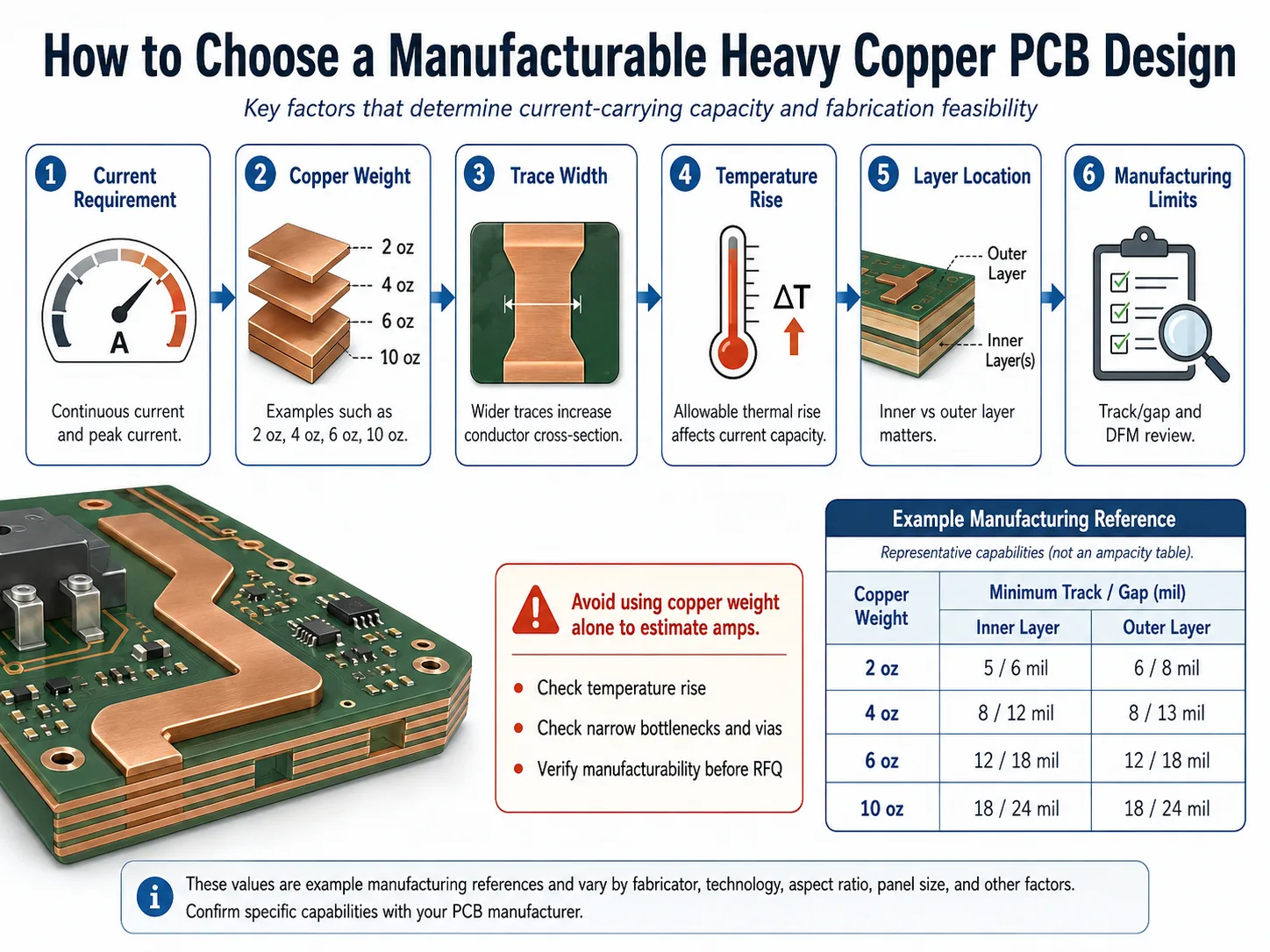
Match Copper Weight to Real Track/Gap Manufacturing Limits
Before releasing a heavy copper layout, compare the selected copper weight against the fabricator’s actual inner- and outer-layer capabilities. UMEC’s heavy copper PCB manufacturing capabilities publish different track/gap values for copper weights from conventional ranges into heavy-copper constructions, with inner-layer values listed through 12 oz and outer-layer values through 15 oz.
The key purchasing question is therefore not simply, “Can this supplier make a 6 oz PCB?” It is, “Can this supplier make the required 6 oz copper while preserving the minimum track and spacing in this specific layout?”
That distinction can prevent a common procurement problem: receiving a technically attractive quotation for a copper weight that requires substantial changes to the released design.
What Should You Confirm Before Ordering a Heavy Copper PCB?
Once the electrical approach has been selected, procurement should confirm that the supplier is evaluating the actual board rather than copper weight alone.
A useful RFQ or DFM package should identify the required continuous current and any relevant peak-current conditions, selected inner- and outer-layer copper weights, minimum trace and spacing requirements, stackup, finished board requirements, operating conditions, fabrication files, and target quantity. Also clearly state any project-specific thermal limits.
What to Include in a Heavy Copper PCB DFM or RFQ Package
The purpose of the package is to let engineering and manufacturing teams evaluate the same design assumptions. If the electrical engineer calculated current capacity using one trace width while the production file contains a narrower neck-down section, the discrepancy should be found before fabrication.
Gerber or other relevant manufacturing files should therefore accompany the key electrical and mechanical requirements. Identify missing assumptions rather than replacing them with generic current tables.
How to Evaluate a Heavy Copper PCB Supplier for a High-Current Design
Supplier selection should focus on evidence relevant to the actual PCB: available copper weights, inner- and outer-layer track/space capability, ability to review the proposed stackup, and willingness to flag manufacturability risks before production.
SZ UMEC CO., LTD publishes dedicated heavy copper, multilayer, and PCB design information rather than presenting heavy copper solely as a generic PCB option. Its heavy copper product page provides copper-dependent track/gap data that engineers and buyers can compare with their layout before requesting production.
Conclusion
Heavy copper PCB current capacity cannot be reduced to a single amperage for each copper weight. The more useful design question is whether the combination of copper weight, trace width, layer location, temperature rise, and complete current-path geometry is suitable for the required load.
Start with the real continuous and peak current, establish the thermal limits, determine how much trace width is available, and then select copper weight. After that, compare the design with the supplier’s track/gap and multilayer manufacturing limits. This sequence reduces the risk of choosing a copper specification that works electrically but forces an avoidable layout change during fabrication.
For a project that has reached the DFM or sourcing stage, contact UMEC with the PCB files, copper requirements, stackup, trace/space dimensions, quantity, application, and relevant operating conditions. That information gives the manufacturing team a more useful basis for reviewing feasibility than copper weight alone. UMEC’s contact page supports PCB file submission for quotation requests.
Heavy Copper PCB Current Capacity FAQs
How much current can a 2 oz copper PCB carry?
There is no universal amp rating for a 2 oz PCB. Current capacity depends on trace width, whether the conductor is internal or external, allowable temperature rise, and operating conditions. Current calculations should use the actual geometry, not copper weight alone.
Does doubling copper weight double PCB current capacity?
Not necessarily. Increasing copper thickness increases conductor cross-section, but current capacity depends on more than copper weight. Trace width, heat dissipation, layer position, ambient conditions, and temperature limits must also be considered.
Is a wider trace better than heavier copper for high current?
A wider trace can be practical when sufficient board area is available. Heavy copper becomes more relevant when space is restricted or when widening traces alone cannot meet the electrical and thermal requirements. UMEC identifies space-constrained high-current designs as a typical reason for using heavy copper.
Can internal and external PCB traces carry the same current?
They should not be treated as equivalent by default. Their thermal environments differ, so include layer position when calculating current-carrying capacity. The manufacturing limits for inner and outer heavy-copper layers may also differ.
What copper weight should be used for a high-current PCB?
Start with required continuous and peak current, allowable temperature rise, available trace width, and layer position. Select a copper weight from those requirements, then verify that the resulting track and spacing can be manufactured. Avoid choosing an oz value before defining the electrical and thermal conditions.