
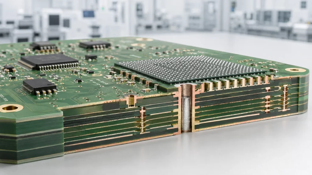
 When purchasers ask why HDI PCB cost more than standard multilayer PCB, the answer is seldom “more layers.” Several factors contribute to the HDI PCB cost, including microvia, sequential lamination, via fill, fine lines/spaces, complex stackup, materials used, inspection required, and the potential for high cost due to tight routing density. The question here is not only how much an HDI PCB costs, but also what must be included in the design, what must not be included because it does not add value, and what must be evaluated before proceeding from prototype to production.
Why HDI PCB Cost Is Higher Than Standard PCB Cost
When a standard through-hole or multilayer construction can no longer accommodate the density or routing required for the product, then an HDI PCB must be considered. Fine-pitch ball grid arrays (BGAs), compact modules, high-speed connectivity, wearables, industrial controls, medical electronics, and communications are technologies that may drive HDI adoption.The increase in cost is related to the need for tighter process control on the board; HDI boards do not always cost more just because they are HDI.
A standard PCB may depend mainly on mechanical drilling, conventional lamination, and wider routing rules. An HDI PCB often adds laser-drilled microvias, blind and buried vias, filled or capped via-in-pad structures, thinner dielectrics, and additional imaging and plating steps. Each added process increases handling, inspection, and registration control requirements, as well as the potential for scrap.
Layer Count Is Only the Starting Point
A 10-layer standard PCB and a 10-layer HDI PCB can have very different pricing. The HDI version may require a 1+N+1 or 2+N+2 build-up, fine lines, microvias between specific layers, and controlled impedance across dense signal paths. That means the supplier must evaluate not only layer count, but also stackup, via structure, minimum trace/space, annular ring, surface finish, material selection, and assembly requirements.
For procurement teams comparing quotes, this distinction matters. A lower quote may be based on assumptions that do not match the actual design file. Before choosing a supplier, buyers should confirm whether the quote includes all microvia, via filling, stackup, impedance, and inspection requirements.
Design Density, Yield Risk and Process Control
HDI manufacturing cost increases when design features approach the edge of a fabricator’s stable process window. Narrow trace/space, small pads, high via counts, tight registration, and complex buried interconnects can reduce manufacturing yield. Even when a design is technically manufacturable, repeated rework, additional inspection, or lower panel yield can raise the final price.
A practical DFM review should identify which cost drivers are necessary for performance and which can be adjusted. This is where early collaboration matters. UMEC supports custom PCB manufacturing projects in which design, fabrication, component sourcing, assembly, and testing requirements may need to be evaluated together rather than treated as separate purchasing steps.
Microvias: A Major Driver of HDI PCB Cost
Microvias allow dense routing between adjacent layers and are often essential for fine-pitch BGA escape routing. They are usually formed by laser drilling rather than mechanical drilling, then plated to create an electrical connection. The cost depends on microvia size, count, location, layer pairing, aspect ratio, whether they are stacked or staggered, and whether they need to be filled.
Why Microvias Increase Fabrication Cost
Microvia PCB cost comes from precision, repetition, and inspection. Laser drilling requires accurate energy control, clean via formation, and proper registration to the target pad. Plating must create a reliable connection without voids or weak points. If the design has many microvias, the cost increase is not only from the holes themselves, but also from process time, quality control, and yield management.
Microvias are appropriate when routing density, board size, or component pitch requires them. They are less suitable when the same routing goal can be reached with conventional vias, wider board area, or a simpler stackup. Engineers should confirm whether every microvia layer is required, especially during early layout review.
Stacked vs Staggered Microvias: Cost and Reliability Trade-Offs
Stacked microvias can support very dense interconnects, especially under fine-pitch components, but they usually demand tighter process control and may require via filling and planarization between build-up steps. Staggered microvias are often easier to manufacture and may reduce costs when routing space allows.
The decision should not be based solely on price. Stacked structures may be necessary for extremely compact designs, but they should be justified by BGA pitch, escape routing, signal path, or mechanical constraints. For cost-sensitive projects, engineers should ask whether staggered microvias, adjusted routing layers, or a modified fanout strategy can meet the same requirement with lower manufacturing risk.
Sequential Lamination: Why Each Build-Up Step Adds Cost
Sequential lamination is one of the most important HDI PCB cost factors. Instead of laminating the full multilayer board in a single main cycle, HDI structures may require repeated cycles of lamination, drilling, plating, imaging, and inspection. More build-up steps usually mean more processing time and more opportunities for registration or yield issues.
How 1+N+1, 2+N+2 and 3+N+3 Affect Pricing
A 1+N+1 HDI stackup generally has one build-up layer on each side of the core. A 2+N+2 or 3+N+3 structure adds more build-up layers and more sequential processes. As the stackup becomes more complex, manufacturing costs and lead times may increase because each stage must align correctly with the previous layers. Simplifying the stackup from 2+N+2 to 1+N+1 can reduce bare board costs by approximately 15-25%.
The right stackup depends on component density, signal requirements, board thickness, mechanical constraints, and reliability expectations. A design with fine-pitch BGAs, a high I/O count, or dense power routing may require more build-up layers. However, a layout should not automatically move to a higher HDI structure without first checking whether routing can be improved.
When a Simpler Stackup Can Reduce Cost
A simpler stackup can reduce HDI PCB manufacturing costs by lowering lamination cycles, reducing stacked microvias, improving panel yield, or relaxing unnecessary tolerances. Engineers must be able to adjust BGA fanout, redistribute routing layers, slightly increase board size, change via placement, or separate high-density and low-density routing zones.
The next step is to send the stackup, Gerber or ODB++ files, critical component information, and target production quantity for DFM review. Early review can prevent a design from being locked into a cost-heavy structure that could have been avoided.
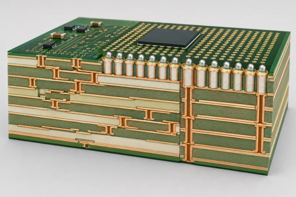
Via Filling and Via-in-Pad: When the Extra Cost Is Necessary
Via filling and via-in-pad are common in HDI designs, especially under BGAs and dense SMT components. They add cost because the via may need to be filled, cured, planarized, capped, and plated over to create a flat solderable pad. Skipping this step may reduce the quote, but it can introduce assembly and reliability risks.
Why Filled and Capped Vias Matter Under BGA Pads
An open or inadequately filled via in a via-in-pad under a BGA causes issues such as solder wicking, voids, and inconsistent solder joints. The filling and capping of the vias form a stable solder plane while enabling dense routing.
This requirement applies primarily to fine-pitch BGAs, HDI modules, dense consumer products, and industrial control circuit boards, among others. It does not apply in cases where the vias are external to the pad or cases where there is sufficient routing space for normal fanout.
Conductive vs Non-Conductive Filling: What Buyers Should Confirm
Via filling material and method should be selected based on electrical, thermal, mechanical, and assembly needs. Conductive filling must be considered when thermal or electrical performance is important. In contrast, non-conductive filling is commonly used for structural support and soldering stability in many via-in-pad designs. The correct choice should be verified against the product specification and application environment.
Before placing an order, buyers should confirm whether the quote includes filled, capped, and plated-over vias; which vias require filling; and whether the filling requirement applies to microvias, through-vias, or both.
DFM Tips to Reduce HDI PCB Cost Before Quotation
The strongest point for cost control is before the layout is frozen. Once the stackup, BGA fanout, via structure, and material choices are fixed, many cost-saving options become harder to apply.
Avoid Over-Specifying Tolerances, Materials and Via Structures
Some HDI boards are over-specified because the layout carries conservative assumptions from earlier designs. Examples include using stacked microvias where staggered structures would suffice, applying via-in-pad to more locations than necessary, selecting tighter trace/space than the routing actually requires, or specifying materials beyond the product’s electrical and thermal needs.
Cost reduction does not mean weakening the design. It means identifying where specifications are essential and where they can be reviewed. For example, impedance, dielectric thickness, copper weight, and surface finish should be matched to the application rather than copied from unrelated projects.
Use DFM Review Before Freezing the Layout
A useful HDI PCB DFM review should assess stackup feasibility, microvia structure, minimum trace/space, via-filling requirements, BGA escape routing, panel utilization, and assembly risks. It should also identify which design changes could reduce cost without creating reliability concerns.
For projects involving HDI boards, PCB assembly, and component sourcing, More Than PCB can be a relevant working model because costs and risks are often distributed across the entire electronics build, not only the bare board.
HDI PCB RFQ Checklist for Accurate Cost Evaluation
An accurate HDI PCB quote depends on complete technical information. Missing details can lead to low initial pricing followed by engineering questions, revised quotes, or production delays.
| RFQ Information | Why It Affects HDI PCB Cost |
| Gerber or ODB++ files | Shows real routing density, copper features, and manufacturability |
| Stackup requirement | Determines lamination cycles, dielectric choices, and layer pairing |
| Via structure | Identifies microvias, buried vias, via-in-pad, and filled vias |
| Minimum trace/space | Affects process difficulty and yield risk |
| Material and Tg requirement | Influences cost, availability, and suitability for performance. |
| Surface finish | Affects solderability, storage, assembly, and cost |
| Quantity and production stage | Prototype, pilot run, and mass production have different cost logic. |
| Assembly requirement | Helps evaluate whether bare board decisions create PCBA risks |
When requesting a quotation, buyers should include drawings, target quantity, application conditions, key components, BGA pitch if relevant, impedance requirements, and any known reliability expectations. For HDI projects requiring fabrication support, HDI PCB manufacturing capabilities should be reviewed together with DFM feedback.
How to Choose an HDI PCB Supplier for Cost Control and Reliability
A qualified HDI PCB supplier should do more than return a number. The supplier should review whether the design can be built consistently, whether the stackup is appropriate, whether via filling is required, and whether a lower-cost alternative can meet the same function.
What a Qualified HDI PCB Supplier Should Review Before Quoting
Before quoting, the supplier should evaluate microvia placement, stacked or staggered via structures, sequential lamination steps, fine-line/space limits, via-filling requirements, BGA fanout, material selection, copper weight, surface finish, and assembly constraints. If a quote does not address these items, the price may not reflect the real manufacturing requirement.
Why One-Stop Engineering Support Matters for HDI Projects
HDI cost control often requires coordination between layout design, PCB fabrication, component sourcing, and assembly. A change that reduces bare board cost may create assembly risk, while a design improvement during layout may reduce both manufacturing complexity and time spent on engineering revisions.
UMEC supports PCB fabrication, PCB design and layout, component sourcing, PCB assembly, and testing-related project needs. For B2B buyers managing complex HDI products, this connected workflow can help clarify cost drivers before production decisions are locked. Technical teams can use Contact UMEC to submit Gerber files, stackup requirements, material preferences, quantity, assembly needs, and application details for review.
Conclusion
HDI PCB cost is mainly driven by microvias, sequential lamination, via filling, via-in-pad, stackup complexity, fine line/space, material selection, and DFM risk. The most practical way to control cost is not to remove every advanced feature, but to confirm which features are truly required for routing, assembly, reliability, and product performance.
UMEC provides DFM review for HDI projects. For an accurate HDI PCB quote, prepare Gerber or ODB++ files, stackup, via structure, materials, surface finishes, quantities, key components, and assembly requirements. A supplier can explain which design choices affect price and where a safer, more cost-effective option may be available.
FAQs
Why are HDI PCBs more expensive than standard PCBs?
HDI PCBs are more expensive because they may require laser-drilled microvias, sequential lamination, fine trace/space, filled or capped vias, tighter registration, and more inspection. The cost depends on the design structure and should be reviewed from the actual files.
Does via filling increase PCB cost?
Yes. Via filling adds extra process steps such as filling, curing, planarization, and plating when required. However, in via-in-pad, fine-pitch BGA, or dense HDI PCB designs, filled and capped vias must be necessary to reduce soldering and reliability risks.
How can engineers reduce HDI PCB cost before fabrication?
Engineers can reduce HDI PCB cost by reviewing whether stacked microvias are necessary, simplifying the stackup where possible, avoiding unnecessary tight tolerances, confirming material requirements, and requesting DFM feedback before finalizing the layout.
What should buyers send for an accurate HDI PCB quote?
Buyers should send Gerber or ODB++ files, stackup, via structure, minimum trace/space, material requirements, surface finish, quantity, impedance requirements, key component information, and whether PCB assembly is needed.
Is the cheapest HDI PCB quote the safest option?
Not necessarily. A low quote may exclude via filling, special stackup requirements, impedance control, or assembly-related risks. Buyers should compare what is included in the technical scope, not only the unit price.